background image

1

SERVICE MANUAL

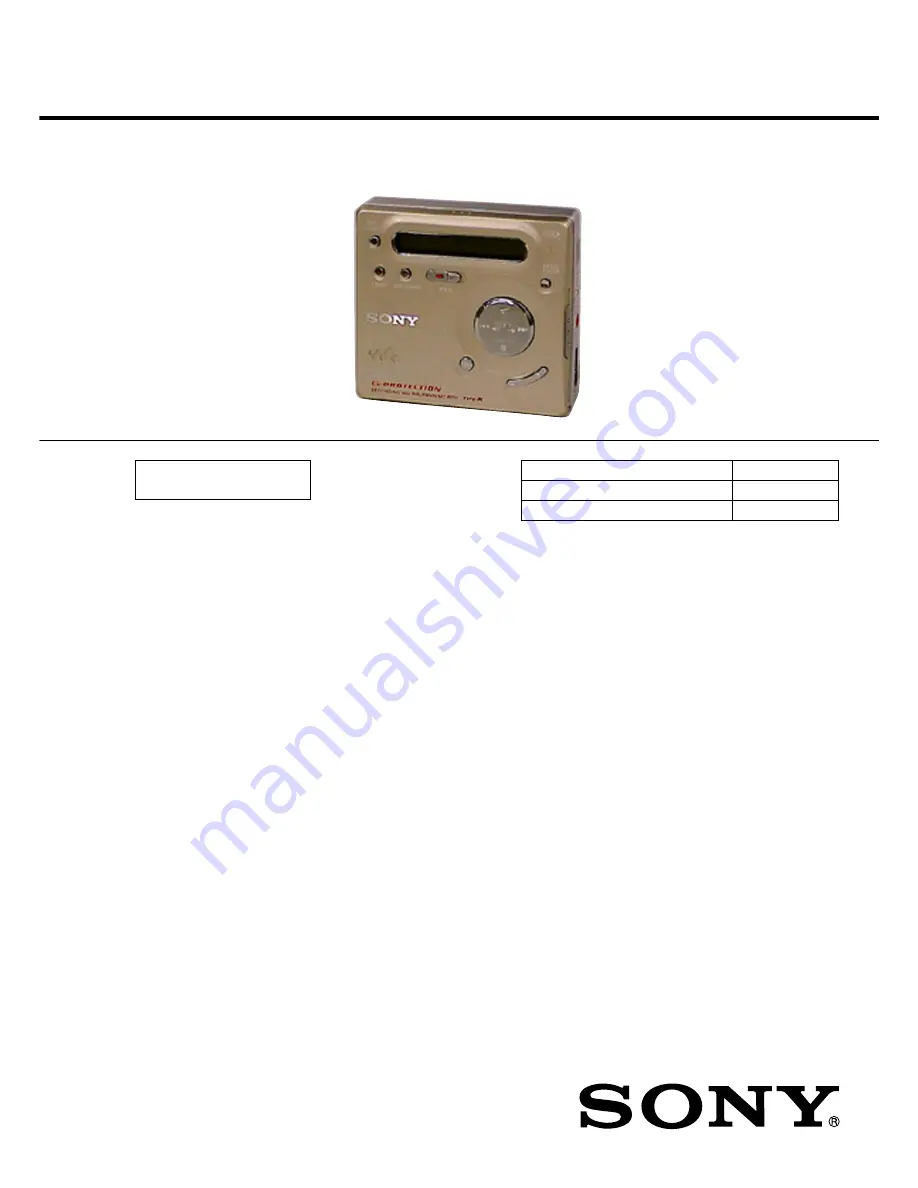
PORTABLE MINIDISC RECORDER

Model Name Using Similar Mechanism

MZ-G750/R700

Mechanism Type

MT-MZR700-172

Optical Pick-up Name

LCX-4R

MD recorder
Audio playing system

MiniDisc digital audio system

Laser diode properties

Material: GaAlAs MQW
Wavelength: 

λ

 = 790 nm

Emission duration: continuous
Laser output: less than 44.6 

µ

W

(This output is the value measured at a
distance of 200 mm from the lens surface
on the optical pick-up block with 7 mm
aperture.)

Recording and playback time

When using MDW-80

Maximum 160 min. in monaural
Maximum 320 min. in stereo

Revolutions

350 rpm to 2,800 rpm (CLV)

Error correction

ACIRC (Advanced Cross Interleave Reed
Solomon Code)

Sampling frequency

44.1 kHz

Sampling rate converter

Input: 32 kHz/44.1 kHz/48 kHz

Coding

ATRAC (Adaptive TRansform Acoustic
Coding)
ATRAC3-LP2
ATRAC3-LP4

SPECIFICATIONS

Modulation system

EFM (Eight to Fourteen Modulation)

Number of channels

2 stereo channels
1 monaural channel

Frequency response

20 to 20,000 Hz ± 3 dB

Wow and Flutter

Below measurable limit

Inputs

Microphone: stereo mini-jack, minimum
input level 0.35 mV
Line in: stereo mini-jack, minimum input
level 49 mV
Optical (Digital) in: optical (digital) mini-
jack

Outputs

i

: stereo mini-jack, maximum output level

5 mW + 5 mW, load impedance 16 ohm

General
Power requirements

Sony AC Power Adaptor (supplied)
connected at the DC IN 3 V jack:

240 V AC, 50 Hz (Australian model)
220 V AC, 50 Hz (EE, CH, AR model)
230-240 V AC, 50 Hz (HK model)
100-240 V AC, 50/60 Hz (E model)

Nickel cadmium rechargeable battery
NC-WMAA (supplied)
LR6 (size AA) alkaline battery (not
supplied)

• Abbreviation

EE

: East European model

CH

: Chinese model

HK

: Hong Kong model

AR

: Argentine model

– Continued on next page –

US and foreign patents licensed
from Dolby Laboratories.

Ver 1.0  2001. 01

Ver 1.0  2002. 05

Sony Corporation

Personal Audio Company

Published by Sony Engineering Corporation

9-874-004-01

2002E0400-1

© 2002. 05

E Model

MZ-R701/R701DPC

Australian Model

East European Model

Chinese Model

MZ-R701

MZ-R701/R701DPC

Summary of Contents for MZ-R701

Page 1: ...er of channels 2 stereo channels 1 monaural channel Frequency response 20 to 20 000 Hz 3 dB Wow and Flutter Below measurable limit Inputs Microphone stereo mini jack minimum input level 0 35 mV Line in stereo mini jack minimum input level 49 mV Optical Digital in optical digital mini jack Outputs i stereo mini jack maximum output level 5 mW 5 mW load impedance 16 ohm General Power requirements Son...

Page 2: ...e to operating conditions the temperature of the location and varieties of batteries 2 Measured value by the standard of JEITA Japan Electronics and Information Technology Industries Association 3 When using a 100 fully charged rechargeable battery 4 When using a Sony LR6 SG STAMINA alkaline dry battery produced in Japan Dimensions Approx 81 28 1 74 4 mm w h d without projections Mass Approx 118 g...

Page 3: ...t Display Mode 16 4 11 Key Check Mode 16 TABLE OF CONTENTS 5 ELECTRICAL ADJUSTMENTS 5 1 Outline 18 5 2 Precautions for Adjustment 18 5 3 Adjustment Sequence 18 5 4 NV Reset 18 5 5 Power Supply Manual Adjustment 19 5 6 Temperature Correction 20 5 7 Laser Power Check 20 5 8 Overall Adjustment Mode 21 5 9 Mode Settings 23 5 10 Resume Clear 23 6 DIAGRAMS 6 1 IC Pin Descriptions 24 6 2 Block Diagram Se...

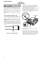
Page 4: ... electrostatic break down sufficiently before the op eration The flexible board is easily damaged and should be handled with care OPTICAL PICK UP FLEXIBLE BOARD In performing the repair with the power supplied to the set removing the MAIN board causes the set to be disabled In such a case fix a convex part of the open close detect switch S806 on MAIN board with a tape in advance Handle the FLEXIBL...

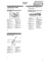
Page 5: ...5 MZ R701 R701DPC SECTION 2 GENERAL This section is extracted from instruction manual ...

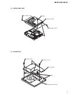
Page 6: ... numerical order given 6 bottom panel assy 4 claw 1 5 2 MI screws 1 4x2 0 3 MI screws 1 4x2 0 3 1 BOTTOM PANEL ASSY Page 6 3 2 UPPER PANEL ASSY Page 7 3 4 MAIN BOARD Page 8 3 6 OP SERVICE ASSY Page 9 SET 3 5 MD MECHANISM DECK Page 8 3 10 DC MOTOR M601 DC MOTOR M603 Page 11 3 8 MOTOR FLEXIBLE BOARD Page 10 3 3 LCD MODULE Page 7 3 7 HOLDER ASSY Page 9 3 9 DC MOTOR M602 Page 10 ...

Page 7: ...7 MZ R701 R701DPC 3 3 LCD MODULE 1 screws 1 7x2 5 4 LCD module claws upper panel B sub assy 2 screws 1 7x2 5 3 3 2 UPPER PANEL ASSY 2 MI screws 1 4x2 0 1 MI screws 1 4x2 0 3 upper panel assy 4 CN804 ...

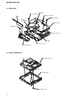
Page 8: ...sy 3 MD mechanism deck boss boss 1 MI screws 1 4x1 6 3 4 MAIN BOARD 3 screws M1 4x2 6 Remove the solders 7 9 Remove the solder q battery case assy qs battery coil spring qd MAIN board qa Remove the solder 4 screws M1 7x3 5 screws M1 4x2 1 CN502 2 arm 8 CN501 ...

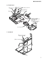
Page 9: ...k spring s 6 thrust detent spring 3 precision pan screw M1 4 5 precision pan screw M1 4 1 washer 0 8 2 5 2 gear SA 8 Pull off the lead screw 7 B A 9 Opening the over write head toward the direction A remove the OP service assy toward the direction B Note Do not open the entire assy forcibly when opening the over write head over write head section ...

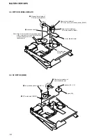
Page 10: ...ve two solders of DC motor over write head up down M603 1 Remove four solders of DC motor sled M602 3 Remove four solders of DC motor spindle M601 DC motor sled circular hole 5 motor flexible board 4 adhesive sheet Note Align a circular hole in the stripping paper with a circular hole in the DC motor sled when mounting the motor flexible board 3 8 MOTOR FLEXIBLE BOARD ...

Page 11: ...n pan screws M1 4 qa gear chassis assy 0 screw M1 2 1 5 9 gear HA 8 gear HB 7 washer 0 8 2 5 2 washer 0 8 2 5 3 gear HC 5 DC moter spindle M601 DC motor over write head up down M603 gear chassis assy gear HA 2 65 mm Note Press fit the gear HA up to the position of the DC motor over write head up down M603 as shown below 3 10 DC MOTOR M601 DC MOTOR M603 ...

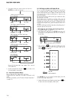
Page 12: ...ted with the chassis etc For test mode set with the method 2 Turn off the power Note If electrical adjustment see page 18 has not been finished completely always start in the test mode The set cannot start in normal mode 4 1 Outline This set provides the Overall adjustment mode that allows CD PB and MO REC PB disk to be automatically adjusted when in the test mode In this overall adjustment mode t...

Page 13: ...key Press the x key Press the N or REC key The key check quits or open the upper panel Press the T MARK or ENTER key for several seconds about 3 seconds ENTER key Test Mode Display Check Mode Servo Adjustment Manual Mode Key Check Mode Audio Adjustment Power Supply Adjustment OP Alignment Adjustment Press the or VOL key Electrical Offset Adjustment Overall Adjustment Mode Sound Skip Check Result D...

Page 14: ...ed with this display the LCD switches to the simple display mode 4 Quit the self diagnosis result display mode and press the x key to return to the test mode display check mode 5 The display changes a shown below each time the ENTER key on the set is pressed However in the power mode item number 700 s only the item is displayed 6 Quit the manual mode and press the x key to return to the test mode ...

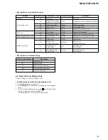
Page 15: ...rror indication codes Problem Indication code Meaning of code Simple display Description No error 00 No error No error 01 Illegal access target Adrs Attempt to access an abnormal address address was specified Servo system error 02 High temperature Temp High temperature 03 Focus error Fcus Disordered focus 04 Spindle error Spdl Abnormal rotation of disc TOC error 11 TOC error TOC Faulty TOC content...

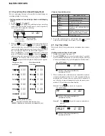
Page 16: ...key is pressed the display item moves up by one then if the REC key is pressed the display in the record mode appears When the REC key is pressed total error count is displayed on the LCD and each time the key is pressed the display item moves down by one as shown below Also if the key is pressed the display item moves up by one then if the N key is pressed the display in the play mode appears Thi...

Page 17: ...red as OK Example2 When the keys on the remote commander are con sidered as OK 5 When all keys were checked or if the upper panel is opened the key check mode quits and the test mode display check mode comes back This set LCD display 0 00 SET OK AD value of the remote commander key hexadecimal OO to FF This set LCD display 0 00 RMC OK AD value of the remote commander key hexadecimal OO to FF ...

Page 18: ...rticular description in the text indicates a set key For the LCD display the LCD display on the set is shown 5 2 Precautions for Adjustment 1 Adjustment must be done in the test mode only After adjusting release the test mode 2 Use the following tools and measuring instruments CD disc TDYS 1 Check MD disc Part No 4 963 646 01 MO disk SONY MD disc available on the market Digital voltmeter Laser pow...

Page 19: ...ted value 2 Vc PWM Duty H adjustment item number 763 3 Vl PWM Duty adjustment item number 764 1 Vc PWM Duty L adjustment item number 762 This set LCD display 0 00 Assy 00 This set LCD display 7 62 VclPWM Adjusted value digital voltmeter MAIN board TP901 VC TP912 GND This set LCD display 7 63 VchPWM Adjusted value digital voltmeter MAIN board TP901 VC TP912 GND This set LCD display 7 64 Vl PWM Adju...

Page 20: ...de item number 011 5 Check that the laser power meter reading is 0 81 0 08 mW 6 Check that the voltage both ends TP and TP of resis tor R521 at this time is below 44 mV This set LCD display 0 14 SetTmp Adjusted value This set LCD display 0 12 HrefPw Adjusted value This set LCD display 0 13 WritPw Adjusted value digital voltmeter MAIN board TP TP laser power meter Optical pick up objective lens Thi...

Page 21: ...nt must be made with no disc loaded 1 Make sure that the power supply voltage is 3V 2 Set the test mode see page 12 3 Press the or VOL key to activate the overall adjustment mode 4 Press the ENTER key 5 Electrical offset adjustment is over if the following display appears This set LCD display 0 00 Assy Disc mark At end power supply adjustment Outside lit At end of electrical offset adj inside lit ...

Page 22: ...ng executed This set LCD display 0 00 NG OF NG item number This set LCD display 0 00 MO OK Overall CD and MO adjustment items 1 Overall CD adjustment items Item No Description 312 313 CD electrical offset adjustment 314 321 CD tracking error gain adjustment 328 CD TWPP gain adjustment 324 CD tracking error offset adjustment 332 336 CD ABCD gain adjustment 344 CD focus gain adjustment 345 CD tracki...

Page 23: ...ust with the VOL key adjusted value up or VOL key adjusted value down so that the adjusted value becomes S30 3 Press the X key Check method of auto time stamp mode 1 Turn the power off and then on 2 Insert a disc and press the X key and REC key at the same time Verify that REC is flashing on the LCD display and then push the MENU ENTER key 3 Press the key four times 4 Press the MENU ENTER key 5 Ve...

Page 24: ... PD NI I Light amount monitor input terminal non invert input 20 PD O O Light amount monitor output terminal 21 ADIP O ADIP duplex FM signal 22 05 kHz 1 kHz output to the system controller IC801 22 DVDD Power supply terminal 2 3 V digital system 23 SBUS I O SSB serial data input output with the system controller IC801 24 SCK I SSB serial clock signal input from the system controller IC801 25 XRST ...

Page 25: ...584 MHz input terminal 25 OSCO O System clock 45 1584 MHz output terminal 26 VSIOSC Ground terminal for OSC cell 27 DAVDD Power supply terminal for the built in D A converter 2 4 V 28 VREFL I Reference voltage input terminal for the internal D A converter L CH 29 AOUTL O Built in D A converter L CH output terminal 30 AOUTR O Built in D A converter R CH output terminal 31 VREFR I Reference voltage ...

Page 26: ...ut from RF amp IC501 75 F0CNT O Filter cut off control signal output Not used open 76 DIFVDD0 Power supply terminal for DSP I F 2 3 V 77 DIFVSS0 Ground terminal for DSP I F 78 APCREF O Control signal output to the reference voltage generation circuit for the laser automatic power control 79 LDDR O PWM signal output for the laser automatic power control Not used open 80 TRDR O Tracking servo drive ...

Page 27: ...munication 2 8 V 142 RMC DTCK I O TSB serial data input output with the remote commander attached headphone 143 TSB SLV VDD Power supply terminal for I F to TSB slave communication 2 3 V 144 TSB SLVI I TSB slave signal input from the remote commander attached headphone fixed at L 145 TSB SLVO O TSB slave signal output from the remote commander attached headphone Not used open 146 TDI I Data input ...

Page 28: ...192 XJACK DET I LINE IN plug detection signal input terminal 193 XMIC DET I Microphone plug detection signal input terminal 194 195 PD S0 1 O PD IC mode changeover signal output to the optical pick up 196 MIFVDD2 Power supply terminal for the microcomputer I F block 2 3 V 197 to 199 MODE1 to 3 O Power supply control signal output for the over write head drive to the over write head drive IC601 200...

Page 29: ...233 SLD MON I Sled servo monitor signal input from the motor driver IC551 234 VLON O Power supply control signal output for the laser diode drive to the power control IC901 235 SLEEP O System sleep control signal coutput to the power control IC901 H sleep ON 236 FFCLR O Input latch output for the start switching to the power control IC901 237 CHG GAIN O Charge gain control signal output to the pow...

Page 30: ...30 MZ R701 R701DPC MEMO ...

Page 31: ...37 27 102 166 88 48 4 87 223 53 3 SPINDLE VOLTAGE MONITOR 52 46 89 44 2 90 220 SPINDLE MOTOR DRIVE 51 54 55 56 1 CHARGE PUMP1 37 42 28 27 31 30 4 EFM PRE DRIVER OVER WRITE HEAD DRIVE Q604 605 HI BRIDGE PRE DRIVER 199 198 197 201 200 1 2 3 5 6 M603 OVER WRITE HEAD UP DOWN OPTICAL PICK UP BLOCK LCX 4R 7 8 11 12 13 3 4 5 6 1 2 14 15 DIN1 ADDT AUDIO SECTION 1 CLK VREF SYSTEM CONTROL POWER SECTION 2 1 ...

Page 32: ...N1 1 OPTICAL RECEIVER J301 LINE IN OPTICAL J303 MIC PLUG IN POWER LINE IN JACK J302 F801 i RVDD DTCK KEY R RGND X801 45 1584MHz SDI0 SDO0 SCK0 SDI0 SDO0 SCK0 SI0 XBCK XCS NV LRCK XCS ADA XPD ADA OSCI OSCO FS256 AOUTL AOUTR XOPT CTL OPT DET XJAC DET MUTE XHP STBY RMC DTCK VREF IN OUTB BEEP OUT R OUTA BEEP OUTL XMIC DET BEEP MUTE STBY BEEP SO0 SCK0 SYSTEM CONTROLLER DIGITAL SIGNAL PROCESSOR 16M BIT ...

Page 33: ...AUX LCD STB XCS LCD PAUSE KEY SET KEY1 SET KEY2 XHOLD SW OPEN CLOSE SW PROTECT XTEST AUXI VB MON TSB MST VDD VL PWM VC PWM XRST CHG MON CHG GAIN CHG HIDC MON GND SW CLK SEL R1040 R1046 R1024 R1025 R1036 L801 VC S806 OPEN CLOSE DETECT S803 PROTECT DETECT SL801 TEST VIF B VB B CN801 SDO0 SCK0 RST STB CS REC XWK1 HOLD DVDD PAUSE SET KEY1 SET KEY2 VIF B R1027 6 VL LASER APC CIRCUIT B L904 CLK CLK SEL ...

Page 34: ...810 C811 C827 C823 L802 C804 R836 L551 C104 C204 L902 L901 L601 C630 FB804 FB802 R1040 R1025 1 1 3 5 7 2 4 6 8 5 8 4 1 D603 R607 R619 R602 C926 C919 R601 D601 Q601 C920 R915 C602 56 50 45 43 5 10 15 20 25 28 29 35 40 42 IC551 IC804 B C E AP830 TP603 AP907 AP831 1 4 8 5 1 5 10 15 20 R815 R831 C521 R830 G D S RVCC DTCK KEY R RGND 11 11 S806 OPEN CLOSE DETECT TP TP 1 679 264 6 5 PRINTED WIRING BOARD ...

Page 35: ...106 R306 R505 C530 C924 C917 R608 C621 C629 R621 R841 R805 R828 C828 R829 C516 C515 C616 R801 C814 FB801 5 4 1 2 3 G D S C E B AP904 AP909 AP910 AP521 AP517 AP801 AP844 AP602 AP601 AP820 AP834 AP832 AP833 AP816 AP817 AP828 AP606 AP847 AP536 AP511 AP842 AP802 AP532 AP835 TP602 AP829 AP531 AP901 TP611 TP610 AP818 AP902 AP534 AP533 AP815 AP908 4 5 3 2 1 1 5 10 14 15 20 25 28 56 50 45 43 42 40 35 29 1...

Page 36: ...ted due to normal produc tion tolerances Waveforms are taken with a oscilloscope Voltage variations may be noted due to normal produc tion tolerances Circled numbers refer to waveforms Signal path E PB j REC ANALOG l REC DIGITAL Note The components identified by mark 0 or dotted line with mark 0 are critical for safety Replace only with part number specified 1 IC5018 IY PB mode 2 IC5019 IX PB mode...

Page 37: ...01 R611 R610 R507 C501 C519 R517 R505 R519 TP TP C604 C602 R601 L601 CN501 CN502 AP501 AP502 AP503 AP504 AP511 AP517 TP505 C518 AP523 AP524 AP532 AP525 AP527 AP535 AP526 SL505 SL506 AP528 AP529 AP530 AP531 AP537 AP536 AP522 AP520 TP605 TP604 C514 C603 C631 TP601 TP602 C627 TP606 AP903 R624 TP610 TP611 AP570 AP571 AP572 AP573 AP574 AP575 AP576 AP577 AP578 AP579 AP554 AP580 AP581 TP603 C632 C628 C62...

Page 38: ...6 FB802 R815 R834 R839 R836 C830 S805 AP833 AP834 AP815 AP816 AP817 C827 AP832 TP801 C809 R803 R802 AP843 AP844 AP845 AP820 AP846 AP847 R837 AP901 AP909 AP908 AP902 C924 C912 C910 C909 AP904 C918 R941 C926 AP907 AP906 R917 R946 C901 R915 IC901 R947 R948 R936 R914 R906 L906 R907 R908 C913 C904 R804 R805 C803 IC805 R841 C828 D803 R835 D904 C902 D901 TP901 TP912 D902 C903 TP902 AP910 R821 C815 C917 C...

Page 39: ...30 R307 C340 C321 R311 F801 R305 R304 L301 C307 C335 C302 C306 C202 C102 C305 C301 TP341 TP342 TP343 TP344 TP345 TP331 TP332 TP333 TP334 TP335 TP336 TP338 TP337 TP339 R111 R211 C308 TP306 TP307 R104 R204 C201 C101 R202 R102 C312 FB302 FB304 TP311 TP312 TP313 TP314 TP315 TP316 TP317 C311 R105 R205 C826 CN801 IC301 D301 D101 D201 FB301 Q301 C212 IC303 Q302 R310 R203 R103 C315 IC302 R1036 R1027 R1040...

Page 40: ...24 23 22 21 20 25 17 16 18 19 VC VC VG VG VC VC VC H BRIDGE CONTROL H BRIDGE CONTROL VC VG VC VC VC VG PRE DRIVER PRE DRIVER VC VC VG VC VG BIAS PGNDW UO PGNDUV WO VMVW VO VMU GND2 CPWI CPVI CPUI COM CPWO CPVO CPUO WI VI UI PWM OE RO1 PGND1 FO1 VM1 RO2 PGND2 FO2 VM12 VM2 FI4 RI4 VM4 FI3 VG VC GND1 PWM24 RI3 FI2 RI2 RI1 FI1 CPAIP CPAIM CPBIM CPBO CPAO CPBIP RO3 PGND3 FO3 VM3 RO4 PGND4 FO4 VM34 IC30...

Page 41: ...TOR VC VG DC IN DC IN DC IN DC IN DC IN VIO VIO VC VC VC VC VC2 VC2 VG VC VG VG2 SW VGC VG3 VG3 VG2 VG VC VG3 IC601 XPC18A22AFCR2 IC901 XPC18A32FCR2 42 41 40 39 38 36 35 34 33 32 31 30 29 37 28 27 26 25 24 23 22 21 20 19 18 17 16 15 14 13 12 11 10 9 8 7 6 5 4 3 2 1 56 55 54 53 52 51 50 49 48 47 46 45 44 43 CLK SLEEP FFCLR VAIFON CLKSEL GND VB VREF RSTREF CRST XRST VC2 VD NC PGND2 PGND2 L2 VL VLO V...

Page 42: ...K Hong Kong model AR Argentine model Ref No Part No Description Remark 7 1 PANEL SECTION Ref No Part No Description Remark R R 1 2 2 3 4 13 14 5 6 2 2 9 6 7 8 10 11 12 not supplied The components identified by mark 0 or dotted line with mark 0 are critical for safety Replace only with part number specified 1 X 3381 858 1 PANEL ASSY UPPER 2 4 218 233 17 SCREW 1 4 MI 3 3 222 892 11 SPRING HOLD TORSI...

Page 43: ...5 3 CHASSIS ASSY SET 52 3 222 779 11 SPRING OPEN TENSION 53 A 3323 650 A MAIN BOARD COMPLETE 54 3 222 780 02 SPRING TORSION 55 4 218 233 11 SCREW 1 4 MI 56 3 335 797 01 SCREW M1 4X2 TOOTHED LOCK 57 3 318 382 01 SCREW 1 7X3 TAPPING 58 3 222 837 01 SPRING BATTERY COIL 59 3 222 838 01 ARM 60 X 3379 899 2 CASE ASSY BATTERY 61 3 242 775 01 SHEET JACK 62 3 243 698 01 CUSHION IC ...

Page 44: ... 1 CHASSIS ASSY 105 4 222 218 02 GEAR HD 106 4 222 223 01 SHAFT SUB 107 4 222 226 01 SPRING EJECT TENSION 108 4 222 222 01 GEAR RACK 109 3 338 645 31 WASHER 0 8 2 5 110 X 3380 408 1 CHASSIS ASSY GEAR 111 3 222 545 01 GEAR HB 112 4 224 885 01 SCREW M1 2X1 5 113 4 222 215 01 GEAR HC 114 1 679 372 11 MOTOR FLEXIBLE BOARD 115 4 963 883 31 SCREW M1 4 PRECISION PAN 116 4 222 216 01 GEAR SA 117 4 222 208...

Page 45: ...49 21 TANTAL CHIP 2 2uF 20 10V C306 1 107 820 11 CERAMIC CHIP 0 1uF 16V C307 1 125 777 11 CERAMIC CHIP 0 1uF 10 10V C308 1 107 820 11 CERAMIC CHIP 0 1uF 16V C309 1 119 923 81 CERAMIC CHIP 0 047uF 10 10V C310 1 125 777 11 CERAMIC CHIP 0 1uF 10 10V C311 1 125 777 11 CERAMIC CHIP 0 1uF 10 10V C312 1 125 889 11 CERAMIC CHIP 2 2uF 10 10V C314 1 135 259 11 TANTAL CHIP 10uF 20 6 3V C315 1 125 837 11 CERA...

Page 46: ...C813 1 125 891 11 CERAMIC CHIP 0 47uF 10 10V C814 1 164 935 11 CERAMIC CHIP 470PF 10 50V C815 1 131 862 11 TANTAL CHIP 47uF 20 4V C816 1 125 777 11 CERAMIC CHIP 0 1uF 10 10V C817 1 125 889 11 CERAMIC CHIP 2 2uF 10 10V C818 1 125 777 11 CERAMIC CHIP 0 1uF 10 10V C819 1 127 772 81 CERAMIC CHIP 0 033uF 10 10V C820 1 127 772 81 CERAMIC CHIP 0 033uF 10 10V C821 1 131 862 11 TANTAL CHIP 47uF 20 4V C822 ...

Page 47: ...501 8 729 922 10 TRANSISTOR 2SA1577 QR Q601 8 729 046 45 FET SI2302DS T1 Q602 8 729 046 44 TRANSISTOR ZDT6718TA Q603 8 729 053 71 FET TS8K1TB Q604 8 729 046 43 FET HAT2051T EL Q605 8 729 046 42 FET HAT2050T EL Q801 8 729 429 44 TRANSISTOR XP1501 RESISTOR R102 1 218 990 11 SHORT CHIP 0 R103 1 218 967 11 RES CHIP 15K 5 1 16W R104 1 218 965 11 RES CHIP 10K 5 1 16W R105 1 218 961 11 RES CHIP 4 7K 5 1 ...

Page 48: ...1 METAL CHIP 100 5 1 10W R841 1 218 990 11 SHORT CHIP 0 R902 1 218 985 11 RES CHIP 470K 5 1 16W R903 1 218 957 11 RES CHIP 2 2K 5 1 16W R905 1 218 957 11 RES CHIP 2 2K 5 1 16W R906 1 218 990 11 SHORT CHIP 0 R907 1 218 985 11 RES CHIP 470K 5 1 16W R908 1 218 977 11 RES CHIP 100K 5 1 16W R909 1 218 965 11 RES CHIP 10K 5 1 16W R910 1 218 965 11 RES CHIP 10K 5 1 16W R911 1 218 949 11 RES CHIP 470 5 1 ...

Page 49: ...ONNECTOR OPTICAL CH HK 3 220 749 01 CASE CARRYING E33 AUS CH HK 3 223 571 01 CASE BATTERY CARRYING 3 228 300 01 CASE BELT CLIP CARRYING EE AR 3 232 311 11 MANUAL INSTRUCTION ENGLISH Digital PC Link R701DPC 3 232 311 31 MANUAL INSTRUCTION SPANISH PORTUGUESE TRADITIONAL CHINESE Digital PC Link R701DPC 3 239 283 11 MANUAL INSTRUCTION ENGLISH AUS EE CH 3 239 283 21 MANUAL INSTRUCTION SPANISH PORTUGUES...

Page 50: ...SION HISTORY Clicking the version allows you to jump to the revised page Also clicking the version at the upper on the revised page allows you to jump to the next revised page Ver Date Description of Revision 1 0 2002 05 New ...

Reviews: