
October 2009
Doc ID 13855 Rev 4
1/67
67
STA309A
Multi-channel digital audio processor with DDX
®
Features
8 channels of 24-bit DDX
®
(direct digital
amplification)
>100 dB of SNR and dynamic range
Selectable 32 kHz - 192 kHz input sample rates
6 channels of DSD/SACD input
Digital gain/atten58 dB to -100 dB in
0.5-dB steps
Soft volume update
Individual channel and master gain/attenuation
plus channel trim (-10 dB to +10 dB)
Up to 10 independent 32-bit user
programmable biquads (EQ) per channel
Bass/treble tone control
Pre and post EQ full 8-channel input mix on all
8 channels
Dual independent limiters/compressors
Dynamic range compression
Automode™:
– 5-band graphic EQ
– 32 preset EQ curves (rock, jazz, pop, etc.)
– Automatic volume controlled loudness
– 5.1 to 2-channel downmix
– Simultaneous 5.1- and 2-channel downmix
outputs
– 3 preset volume curves
– 2 preset anti-clipping modes
– Preset movie nighttime listening mode
– Preset TV channel/commercial AGC mode
– 5.1, 2.1 bass management configurations
– 8 preset crossover filters
Individual channel and master soft/hard mute
Automatic zero-detect and invalid input mute
Automatic invalid input detect mute
Advanced PopFree operation
Advanced AM interference frequency
switching and noise suppression modes
I
2
S output channel mapping function
Independent channel volume and DSP bypass
Channel mapping of any input to any
processing/DDX
®
channel
DC blocking selectable high-pass filter
Selectable per-channel DDX
®
damped ternary
or binary PWM output
Max power correction for lower full-power THD
Variable per channel DDX
®
output delay control
192 kHz internal processing sample rate, 24-bit
to 36-bit precision
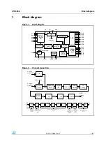
Description
The STA309A is a single chip solution for digital
audio processing and control in multi-channel
applications. It provides output capabilities for
DDX
®
. In conjunction with a DDX
®
power device,
the STA309A provides high-quality,
high-efficiency, all digital amplification. The device
is extremely versatile, allowing inputs of most
digital formats including 6.1/7.1-channel and
192 kHz, 24-bit DVD-audio, DSD/SACD. In 5.1
applications the additional 2 channels can be
used for audio line-out or headphone drive. In
speaker mode, with 8 channel outputs in parallel,
the STA309A can deliver more than 1 W.
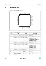
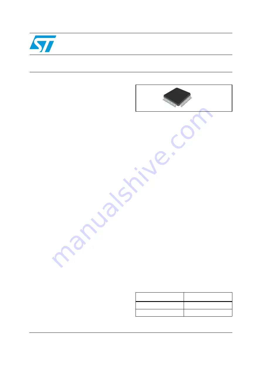
Table 1.
Device summary
Order code
Package
STA309A
TQFP64
STA309A13TR
TQFP64
TQFP64


