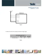
background image


WE865-DUAL Hardware User Guide    

 
1vv0300787 Rev. 1 - 03/10/08     

Summary of Contents for WE865-DUAL

Page 1: ...WE865 DUAL Hardware User Guide 1vv0300787 Rev 1 03 10 08 ...

Page 2: ...ser Guide 1vv0300787 Rev 1 03 10 08 Reproduction forbidden without Telit Communications S p A written authorization All Rights Reserved page 2 of 48 This document is relating to the following products WE865DUA000 001 ...

Page 3: ...2 Shut down mode 15 4 2 Power supply design guidelines 16 4 2 1 5V input source 17 4 2 2 12V input source 18 4 2 3 Battery source 20 4 3 Reset signals 20 4 3 1 Reset 21 4 3 2 Manual reset 22 4 4 SDIO signals 23 5 Thermal design guidelines 24 6 PCB layout design guidelines 25 7 Antenna 26 7 1 Wi Fi antenna guidelines 26 7 2 Wi Fi antenna PCB trace guidelines 27 7 3 Wi Fi antenna installation guidel...

Page 4: ...authorization All Rights Reserved page 4 of 48 9 1 4 Pin table 39 10 Mounting the WE865 DUAL on the application board 40 10 1 Stencil 40 10 2 PCB pad design 40 10 3 Solder paste 43 10 4 Solder reflow 43 11 Moisture sensitivity 45 12 Conformity assessment issues 46 13 Safety recommendations 47 14 Document change log 48 ...

Page 5: ...ng the foregoing Telit does not make any warranty as to the information contained herein and does not accept any liability for any injury loss or damage of any kind incurred by use of or reliance upon the information Telit disclaims any and all responsibility for the application of the devices characterized in this document and notes that the application of the device must comply with the safety s...

Page 6: ...ttuali descritte in questo manuale DE Die integration des Wi Fi WE865 DUAL Moduls in ein Gerät muß gemäß der in diesem Dokument beschriebenen Kunstruktionsregeln erfolgen SL Integracija Wi Fi WE865 DUAL modula v uporabniški aplikaciji bo morala upoštevati projektna navodila opisana v tem piročniku SP La utilización del modulo Wi Fi WE865 DUAL debe ser conforme a los usos para los cuales ha sido de...

Page 7: ...DUAL Product Description 80312ST10046A 2 Telit WE865 DUAL Software User Guide 1vv0300788 3 Telit GE863 PRO Hardware User Guide 1vv0300773a 4 Telit GE863 PRO Software User Guide 1vv0300788 5 Telit GE863PRO3 EVK User Guide 1vv0300776 6 Telit GE863PRO3 Linux SW User Guide 1vv0300781 7 Telit GE863PRO3Linux Development Environment User Guide1vv0300780 All documentation can be downloaded from Telit s of...

Page 8: ...ion forbidden without Telit Communications S p A written authorization All Rights Reserved page 8 of 48 2 Mechanical description The Telit WE865 DUAL module overall dimensions are Length 22 15 mm max Width 22 15 mm max Thickness 3 48 mm max Weight 3 5 g Figure 1 ...

Page 9: ...WE865 DUAL HW User Guide 1vv0300787 Rev 1 03 10 08 Reproduction forbidden without Telit Communications S p A written authorization All Rights Reserved page 9 of 48 Figure 2 Bottom side ...

Page 10: ... O SDIO CMD or SPI MOSI 10KOhm pull up SDIO or SPI Testing and Certification C3 TEST_1 O Test line n 1 TEST C4 TEST_2 I Test line n 2 TEST C5 TEST_3 I Test line n 3 TEST D5 TEST_4 I Test line n 4 TEST Miscellaneous Functions B1 EN_A I Enable shut down 10KOhm pull up control C1 MR_RESET I Manual reset 100KOhm pull up control D1 EN_B I Enable shut down 10KOhm pull up control D2 RESET I Reset for hos...

Page 11: ...ion All Rights Reserved page 11 of 48 Ball Signal I O Function Internal PULL UP DOWN Type A7 N C A8 N C B4 N C B5 N C B6 N C B7 N C B8 N C C5 N C C6 N C C8 N C D3 N C D4 N C D6 N C D7 N C D8 N C E3 N C E4 N C E6 N C E8 N C F4 N C F5 N C F6 N C F7 N C F8 N C G2 N C G6 N C G7 N C G8 N C H1 N C H2 N C H4 N C H7 N C H8 N C Table 1 ...

Page 12: ... 3 2 Ball grid A B C D E F G H 1 SDIO 0 EN_A MR_RESET EN_B VDD VCC_A GND NC 2 SDIO 2 SDIO 1 GND RESET VDD VCC_A NC NC 3 SDIO_CLK SDIO 3 TEST_1 NC NC VCC_A GND GND 4 SDIO_CMD NC TEST_2 NC NC NC GND NC 5 NC NC TEST_3 TEST_4 GND NC GND RF_ANT 6 NC NC NC NC NC NC NC GND 7 NC NC GND NC GND NC NC NC 8 NC NC NC NC NC NC NC NC Table 2 NOTE The drawing above is a top view ...

Page 13: ...quirements and the guidelines that will follow for a proper design 4 1 Power supply Powering of the module wide range voltage operation from 3 4V up to 4 2V typical voltage 3 8V the same as for GE863 PRO3 The above voltage range is chosen in order to use the same voltage range for the Wi Fi module WE865 DUAL and the GE863 PRO3 4 1 1 Unique supply voltage for WE865 DUAL and GE863 PRO3 In order to g...

Page 14: ...t Communications S p A written authorization All Rights Reserved page 14 of 48 Figure 3 The table below shows the operating and absolute voltage ranges VOLTAGE RANGES 25 C Min V Typ V Max V Operating range 3 4 3 8 4 2 Table 4 VCC_A F1 VCC_A F2 VCC_A F3 3 8 V typ VDD E1 VDD E2 WE865 DUAL ...

Page 15: ...ode In order to minimize the current consumption it is possible to completely shut down the WE865 DUAL That is achieved by acting on the relevant signal outside the module which directly acts on the power device enable Shut down signals The shut down is achievable by driving low both the EN_B ball D1 and EN_A ball B1 signals to be connected together As EN_B ball D1 and EN_A ball B1 are internally ...

Page 16: ...sign and it strongly affects the product overall performances hence read carefully the requirements and the guidelines that will follow for a proper design The table below shows the WE865 DUAL operating voltage range VOLTAGE RANGE Nominal Supply Voltage 3 8V Minimum Supply Voltage 3 4V Max Supply Voltage 4 2V Table 8 The electrical design of the power supply strongly depends on the power source th...

Page 17: ...ing a linear regulator a proper heat sink shall be provided in order to dissipate the generated power A protection diode should be inserted close to the power input in order to save the WE865 DUAL from power polarity inversion This can be the same diode as for spike protection The figure below shows a possible solution for the switching power supply It must be taken into account that the power sup...

Page 18: ...esence of peak current load When using a switching regulator 500 kHz switching frequency or more is preferable because of its smaller inductor size and its faster transient response This allows the regulator to respond quickly to any current peak absorption A protection diode should be inserted close to the power input in order to save the WE865 DUAL from power polarity inversion This can be the s...

Page 19: ...WE865 DUAL HW User Guide 1vv0300787 Rev 1 03 10 08 Reproduction forbidden without Telit Communications S p A written authorization All Rights Reserved page 19 of 48 Figure 6 ...

Page 20: ... with Li ION batteries only Using other type of batteries an external charger will be needed The battery capacity should be suitable chosen dependently on the customer s application current consumption and the battery life requirements When integrating the GE863 PRO3 with the WE865 DUAL modules together in the user application the battery capacity must be at least 800mAh in order to withstand any ...

Page 21: ...age 21 of 48 4 3 1 Reset An active high host reset RESET ball D2 allowing the WE865 DUAL to be reset by an external device host This pin is internally pulled down do not drive the signal during normal operation The signal must be asserted for a period greater than 1ms VOLTAGE LEVELS 25 C Min V Max V Remark VIH 2 0 3 0 Table 9 Figure 7 WE865 DUAL RESET ...

Page 22: ...e 22 of 48 4 3 2 Manual reset An active low manual reset MR_RESET ball C1 see the table below for the allowed voltage levels As the pin is internally pulled up do not drive the signal during normal operation The signal must be asserted for a period greater than 1ms VOLTAGE LEVELS 25 C Min V Max V Remark VIL 0 3 0 825 Table 10 Figure 8 WE865 DUAL MR_RESET ...

Page 23: ...e host processor Telit GE863 PRO3 WE865 DUAL SDIO voltage levels are fully compatible with the GE863 PRO3 I O voltage levels 47 Ohm series resistor on each SDIO line and 12pF capacitor on clock line must be inserted in order to avoid noise see Electrical design guidelines chapter Refer to 8 2 Voltage levels for all the SDIO pins are reported in the table VOLTAGE LEVELS 25 C Min V Max V Remark VIL ...

Page 24: ...n authorization All Rights Reserved page 24 of 48 5 Thermal design guidelines The thermal design for the power supply heat sink should be done taking into account the current consumption involved in the appropriate power supply configuration Please refer to 4 1 1 1 for detailed information on the current consumption ...

Page 25: ...ing diode must be as short as possible It is recommended to place the inductor and the diode very close to the power switching IC This is done in order to reduce the radiated field noise of the switching frequency 100 500 kHz usually The use of a good common ground plane is generally suggested The placement of the power supply on the board should be done in such a way to guarantee that the high cu...

Page 26: ... for a Telit WE865 DUAL device ANTENNA REQUIREMENTS Frequency range MHz 2400 2500 Gain dBi 2 Impedance Ohm 50 Maximum Input Power mW 100 VSWR recommended 2 Table 12 Frequency range indicated in order to support 14 Wi Fi channels Smaller ranges are allowed or requested for application over 11 or 13 channels Please refer to IEEE specifications and to the proper regulatory body directives about 802 1...

Page 27: ...or the Ground plane Surround on the sides over and under the antenna line on PCB with Ground avoid having other signal tracks facing directly the antenna line track The ground around the antenna line on PCB has to be strictly connected to the Ground Plane by placing vias once per 2mm at least Place EM noisy devices as far as possible from WE865 DUAL antenna line Keep the antenna line far away from...

Page 28: ...ation guidelines Install the antenna in a place covered by the Wi Fi signal The antenna must be installed to provide a separation distance of at least 20 cm from all persons and must not be co located or operating in conjunction with any other antenna or transmitter Antenna shall not be installed inside metal cases Antenna shall be installed also according Antenna manufacturer instructions ...

Page 29: ... forbidden without Telit Communications S p A written authorization All Rights Reserved page 29 of 48 8 Integration with the GE863 PRO3 Figure 9 Block diagram NOTE It is mandatory to leave available the TEST lines in the customer design TEST_1 TEST_2 TEST_3 TEST_4 ...

Page 30: ...GPIO PC29 ball F5 through a N channel MOSFET In the GE863 PRO3 the power supply inputs of the GSM engine and the ARM processor part have been kept separate VBATT is the input for the GSM part VBATT2 is the input for ARM It is possible to connect together the two power inputs since they have compatible ranges but if it is desired the two power supplies can be kept separate If keeping separated VBAT...

Page 31: ...O interface is available on the WE865 DUAL that must be connected to the host processor Telit GE863 PRO3 The WE865 DUAL SDIO voltage levels are fully compatible with the GE863 PRO3 I O voltage levels 47 Ohm series resistor on each SDIO line and 12pF capacitor on clock line must be inserted in order to avoid noise see Electrical design guidelines chapter Refer to block diagram in Figure 7 Figure 11...

Page 32: ...erface board In such a case the WE865 DUAL module is directly soldered on its interface board The figure below shows how the boards must be assembled in order to allow the system working Figure 12 All the boards are connected each other via 40 pins connectors The core of the evaluation system is the EVK PRO3 EVALUATION KIT which can be split into several functional blocks depending on the implemen...

Page 33: ...ser Guide 1vv0300787 Rev 1 03 10 08 Reproduction forbidden without Telit Communications S p A written authorization All Rights Reserved page 33 of 48 Figure 13 WE865 DUAL interface board WE865 DUAL EVK PRO3 GE863 PRO3 ...

Page 34: ...ser Guide 1vv0300787 Rev 1 03 10 08 Reproduction forbidden without Telit Communications S p A written authorization All Rights Reserved page 34 of 48 Figure 14 EVK PRO3 WE865 DUAL interface board WE865 DUAL GE863 PRO3 ...

Page 35: ...er Guide 1vv0300787 Rev 1 03 10 08 Reproduction forbidden without Telit Communications S p A written authorization All Rights Reserved page 35 of 48 9 1 WE865 DUAL Interface board 9 1 1 Mechanical description Figure 15 ...

Page 36: ...ons S p A written authorization All Rights Reserved page 36 of 48 9 1 2 Main components Main components TOP side list WE865 DUAL module PL101 2 pin jumper PL102 2 pin jumper SW101 Reset button Push to drive MR_RESET low SO104 RF connector alternative to AT101 PL103 5 pin header SPI for test Figure 16 ...

Page 37: ...03 10 08 Reproduction forbidden without Telit Communications S p A written authorization All Rights Reserved page 37 of 48 Main components BOTTOM side list SO101 Interface connector SO102 Interface connector SO103 Interface connector Figure 17 ...

Page 38: ...lit Communications S p A written authorization All Rights Reserved page 38 of 48 9 1 3 Jumpers settings The figure below shows the PL101 and PL102 jumpers on the TOP side in the interface board Figure 18 PL101 Short the jumper to drive EN_A low PL102 Short the jumper to drive EN_B low ...

Page 39: ...ED RESERVED 13 RESERVED RESERVED RESERVED 14 RESERVED RESERVED RESERVED 15 RESERVED RESERVED RESERVED 16 RESERVED RESERVED RESERVED 17 RESERVED RESERVED RESERVED 18 RESERVED RESERVED RESERVED 19 RESERVED RESERVED RESERVED 20 RESERVED RESERVED RESERVED 21 RESERVED RESERVED RESERVED 22 RESERVED RESERVED RESERVED 23 RESERVED RESERVED RESERVED 24 RESERVED RESERVED RESERVED 25 RESERVED RESERVED RESERVE...

Page 40: ...65 DUAL on the application board The Telit WE865 DUAL module has been designed in order to be compliant with a standard lead free SMT process 10 1 Stencil Stencil s apertures layout can be the same of the recommended footprint 1 1 we suggest a thickness of stencil foil 120μm 10 2 PCB pad design Non solder mask defined NSMD type is recommended for the solder pads on the PCB Figure 19 ...

Page 41: ...Reserved page 41 of 48 Figure 20 Recommendations for PCB pad dimensions Dimension Value mm Ball pitch 2 Solder resist opening diameter A 1 150 Metal PAD diameter B 1 0 05 Table 15 Placement of microvias not covered by solder resist is not recommended inside the Solder resist Opening unless the microvia carry the same signal of the pad itself ...

Page 42: ...endations for PCB pad surfaces Finish Layer tickness um Properties Electro less Ni Immersion Au 3 7 0 05 0 15 good solder ability protection high shear force values Table 16 The PCB must be able to resist the higher temperatures which are occurring at the lead free process This issue should be discussed with the PCB supplier Generally the wet ability of tin lead solder paste on the described surfa...

Page 43: ...production forbidden without Telit Communications S p A written authorization All Rights Reserved page 43 of 48 10 3 Solder paste Lead free Solder paste Sn Ag Cu Table 17 10 4 Solder reflow The following is the recommended solder reflow profile Figure 22 ...

Page 44: ...Max Tsmax Time min to max ts 150 C 200 C 60 180 seconds Tsmax to TL Ramp up rate 3 C second max Time maintaned above Temperature TL Time tL 217 C 60 150 seconds Peak Temperature Tp 245 0 5 C Time within 5 C of actual Peak Temperature tp 10 30 seconds Ramp down rate 6 C second max Time 25 C to Peak Temperature 8 minutes max Table 18 NOTE All temperatures refer to topside of the package measured on ...

Page 45: ...take care of the following conditions The shelf life of WE865 inside of the dry bag shall be 12 month from the bag seal date when stored in a non condensing atmospheric environment of 40 C 90 RH Environmental condition during the production 30 C 60 RH according to IPC JEDEC J STD 033A paragraph 5 The maximum time between the opening of the sealed bag and the reflow process shall be 168 Hours if th...

Page 46: ... 1 2006 10 EMC Electromagnetic Compatibility Standards EN 301 489 1 and EN 301 489 17 LVD Low Voltage Directive Standards EN 60 950 The WE865 DUAL module is conform with the following US Directives Use of RF Spectrum Standards FCC 47 Part 15 EMC Electromagnetic Compatibility Standards FCC 47 Part 15 To meet the FCC s RF exposure rules and regulations The system antenna s used for this transmitter ...

Page 47: ...because electrostatic discharges may damage the product itself The system integrator is responsible of the functioning of the final product therefore care has to be taken to the external components of the module as well as of any project or installation issue because the risk of disturbing the external networks or devices or having impact on the security Should there be any doubt please refer to t...

Page 48: ...n D Da at te e C Ch ha an ng ge es s ISSUE 0 20 08 08 Preliminary Release ISSUE 1 03 10 08 Updated mechanical dimensions Updated pin out and ball grid Updated power configuration section Added current consumption Updated reset section Updated antenna section Updated integration section with GE863 PRO3 Updated evaluation kit section Added conformity assessment issues section Added safety recommenda...

Reviews: