background image


64-Bit TX System RISC 

TX49 Family 

TMPR4937 


Rev. 2.0


Summary of Contents for TX49 TMPR4937

Page 1: ...64 Bit TX System RISC TX49 Family TMPR4937 Rev 2 0 ...

Page 2: ...e precautions and conditions set forth in the Handling Guide for Semiconductor Devices or TOSHIBA Semiconductor Reliability Handbook etc The Toshiba products listed in this document are intended for usage in general electronics applications computer personal equipment office equipment measuring equipment industrial robotics domestic appliances etc These Toshiba products are neither intended nor wa...

Page 3: ...croprocessor a discussion of the application fields in which the microprocessor is utilized and an overview of design methods On the other hand the more experienced designer will find complete technical specifications for this product Toshiba continually updates its technical information Your comments and suggestions concerning this and other Toshiba documents are sincerely appreciated and may be ...

Page 4: ......

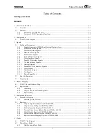
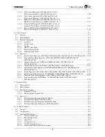
Page 5: ...Signals 3 8 3 1 12 Clock Signals 3 8 3 1 13 Initialization Signal 3 9 3 1 14 Test Signals 3 9 3 1 15 Power Supply Pins 3 9 3 2 Boot Configuration 3 10 3 3 Pin multiplex 3 14 4 Address Mapping 4 1 4 1 TX4937 Physical Address Map 4 1 4 2 Register Map 4 2 4 2 1 Addressing 4 2 4 2 2 Ways to Access to Internal Registers 4 2 4 2 3 Register Map 4 3 5 Configuration Registers 5 1 5 1 Detailed Description 5...

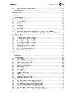
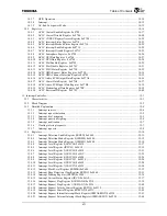
Page 6: ...7 5 9 External ACK Mode Access 32 bit Bus 7 46 7 5 10 READY Mode Access 32 bit Bus 7 52 7 6 Flash ROM SRAM Usage Example 7 54 8 DMA Controller 8 1 8 1 Features 8 1 8 2 Block Diagram 8 2 8 3 Detailed Explanation 8 4 8 3 1 Transfer Mode 8 4 8 3 2 On chip Registers 8 5 8 3 3 External I O DMA Transfer Mode 8 5 8 3 4 Internal I O DMA Transfer Mode 8 8 8 3 5 Memory Memory Copy Mode 8 9 8 3 6 Memory Fill...

Page 7: ... SDRAM 8 53 8 5 14 Single Address Single Transfer from I O to Memory 32 bit SDRAM 8 54 8 5 15 External I O Device SRAM Dual Address Transfer 8 55 8 5 16 External I O Device SDRAM Dual Address Transfer 8 57 8 5 17 External I O Device Non burst SDRAM Dual Address Transfer 8 59 9 SDRAM Controller 9 1 9 1 Characteristics 9 1 9 2 Block Diagram 9 2 9 3 Detailed Explanation 9 3 9 3 1 Supported SDRAM conf...

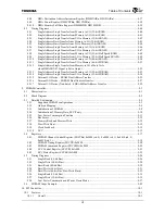
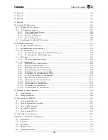
Page 8: ...24 10 35 10 4 11 Subsystem ID Register PCISID 0xD02C 10 36 10 4 12 Capabilities Pointer Register PCICAPPTR 0xD034 10 37 10 4 13 PCI Configuration 2 Register PCICFG2 0xD03C 10 38 10 4 14 G2P Timeout Count Register G2PTOCNT 0xD040 10 39 10 4 15 G2P Status Register G2PSTATUS 0xD080 10 40 10 4 16 G2P Interrupt Mask Register G2PMASK 0xD084 10 41 10 4 17 Satellite Mode PCI Status Register PCISSTATUS 0xD...

Page 9: ...57 Configuration Data 3 Register PCICDATA3 0xD1DC 10 88 10 4 58 PDMAC Chain Address Register PDMCA 0xD200 10 89 10 4 59 PDMAC G Bus Address Register PDMGA 0xD208 10 90 10 4 60 PDMAC PCI Bus Address Register PDMPA 0xD210 10 91 10 4 61 PDMAC Count Register PDMCTR 0xD218 10 92 10 4 62 PDMAC Configuration Register PDMCFG 0xD220 10 93 10 4 63 PDMAC Status Register PDMSTATUS 0xD228 10 95 10 5 PCI Config...

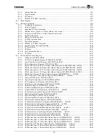
Page 10: ...0xF008 TMCPRA1 0xF108 TMCPRA2 0xF208 12 12 12 4 4 Compare Register Bn TMCPRBn TMCPRB0 0xF00C TMCPRB1 0xF10C 12 13 12 4 5 Interval Timer Mode Register n TMITMRn TMITMR0 0xF010 TMITMR1 0xF110 TMITMR2 0xF210 12 14 12 4 6 Divide Register n TMCCDRn TMCCDR0 0xF020 TMCCDR1 0xF120 TMCCDR2 0xF220 12 15 12 4 7 Pulse Generator Mode Register n TMPGMRn TMPGMR0 0xF000 TMPGMR1 0xF130 12 16 12 4 8 Watchdog Timer ...

Page 11: ...st detection 15 5 15 3 3 Interrupt level assigning 15 5 15 3 4 Interrupt priority assigning 15 6 15 3 5 Interrupt notification 15 7 15 3 6 Clearing interrupt requests 15 7 15 3 7 Interrupt requests 15 8 15 4 Registers 15 10 15 4 1 Interrupt Detection Enable Register IRDEN 0xF600 15 11 15 4 2 Interrupt Detection Mode Register 0 IRDM0 0xF604 15 12 15 4 3 Interrupt Detection Mode Register 1 IRDM1 0xF...

Page 12: ...RAM Interface AC characteristics 21 6 21 5 4 External Bus Interface AC characteristics 21 8 21 5 5 PCI Interface AC characteristics 66 MHz 21 9 21 5 6 PCI Interface AC characteristics 33 MHz 21 9 21 5 7 PCI EEPROM Interface AC characteristics 21 11 21 5 8 DMA Interface AC characteristics 21 11 21 5 9 Interrupt Interface AC characteristics 21 12 21 5 10 SIO Interface AC characteristics 21 13 21 5 1...

Page 13: ...Table of Contents ix TMPR4937 Revision History 1 ...

Page 14: ...Table of Contents x ...

Page 15: ...Handling Precautions ...

Page 16: ......

Page 17: ... specifications Also please keep in mind the precautions and conditions set forth in the TOSHIBA Semiconductor Reliability Handbook The TOSHIBA products listed in this document are intended for usage in general electronics applications computer personal equipment office equipment measuring equipment industrial robotics domestic appliances etc These TOSHIBA products are neither intended nor warrant...

Page 18: ...1 Using Toshiba Semiconductors Safely 1 2 ...

Page 19: ...you move on to the detailed descriptions of the precautions Explanation of labels Indicates an imminently hazardous situation which will result in death or serious injury if you do not follow instructions Indicates a potentially hazardous situation which could result in death or serious injury if you do not follow instructions Indicates a potentially hazardous situation which if not avoided may re...

Page 20: ... a device is on do not touch the device s heat sink Heat sinks become hot so you may burn your hand Do not touch the tips of device leads Because some types of device have leads with pointed tips you may prick your finger When conducting any kind of evaluation inspection or testing be sure to connect the testing equipment s electrodes or probes to the pins of the device under test before powering ...

Page 21: ...t circuit current will flow continuously and the device may break down or burst into flames resulting in fire or injury When incorporating a visible semiconductor laser into a design use the device s internal photodetector or a separate photodetector to stabilize the laser s radiant power so as to ensure that laser beams exceeding the laser s rated radiant power cannot be emitted If this stabilizi...

Page 22: ...ember to take the device s forward and reverse losses into account The leakage current in these devices is greater than that in ordinary rectifiers as a result if a high speed rectifier is used in an extreme environment e g at high temperature or high voltage its reverse loss may increase causing thermal runaway to occur This may in turn cause the device to explode and scatter shrapnel resulting i...

Page 23: ...ls in the working area are grounded to earth Place a conductive mat over the floor of the work area or take other appropriate measures so that the floor surface is protected against static electricity and is grounded to earth The surface resistivity should be 104 to 108 Ω sq and the resistance between surface and ground 7 5 105 to 108 Ω Cover the workbench surface also with a conductive mat with a...

Page 24: ...rs boxes jigs or bags that are made of anti static materials or materials which dissipate electrostatic charge Make sure that cart surfaces which come into contact with device packaging are made of materials which will conduct static electricity and verify that they are grounded to the floor surface via a grounding chain In any location where the level of static electricity is to be closely contro...

Page 25: ...es and packaging materials with care To avoid damage to devices do not toss or drop packages Ensure that devices are not subjected to mechanical vibration or shock during transportation Ceramic package devices and devices in canister type packages which have empty space inside them are subject to damage from vibration and shock because the bonding wires are secured only at their ends Plastic molde...

Page 26: ... If devices have been stored for more than two years their electrical characteristics should be tested and their leads should be tested for ease of soldering before they are used 3 2 2 Moisture proof packing Moisture proof packing should be handled with care The handling procedure specified for each packing type should be followed scrupulously If the proper procedures are not followed the quality ...

Page 27: ...mperature which it can withstand bake at 125 C for 20 hours Some devices require a different procedure Tube Transfer devices to trays bearing the Heatproof marking or indicating the temperature which they can withstand or to aluminum tubes before baking at 125 C for 20 hours Tape Deviced packed on tape cannot be baked and must be used within the effective usage period after unpacking as specified ...

Page 28: ...ge or current on any pin exceeds the absolute maximum rating the device s internal circuitry can become degraded In the worst case heat generated in internal circuitry can fuse wiring or cause the semiconductor chip to break down If storage or operating temperatures exceed rated values the package seal can deteriorate or the wires can become disconnected due to the differences between the thermal ...

Page 29: ...ss voltage may have been applied only for an instant the large current continues to flow between Vcc Vdd and GND Vss This causes the device to heat up and in extreme cases to emit gas fumes as well To avoid this problem observe the following precautions 1 Do not allow voltage levels on the input and output pins either to rise above Vcc Vdd or to fall below GND Vss Also follow any prescribed power ...

Page 30: ... θca Tc Ta P in which θja thermal resistance between junction and surrounding air C W θjc thermal resistance between junction and package surface or internal thermal resistance C W θca thermal resistance between package surface and surrounding air or external thermal resistance C W Tj junction temperature or chip temperature C Tc package surface temperature or case temperature C Ta ambient tempera...

Page 31: ...g on the types of device used To protect against noise lower the impedance of the pattern line or insert a noise canceling circuit Protective measures must also be taken against surges For details of the appropriate protective measures for a particular device consult the relevant databook 3 3 12 Electromagnetic interference Widespread use of electrical and electronic equipment in recent years has ...

Page 32: ...device insulation Such requirements must be fully taken into account to ensure that your design conforms to the applicable safety standards 3 3 15 Other precautions 1 When designing a system be sure to incorporate fail safe and other appropriate measures according to the intended purpose of your system Also be sure to debug your system under actual board mounted conditions 2 If a plastic package d...

Page 33: ...package lead insertion and surface mount During mounting on printed circuit boards devices can become contaminated by flux or damaged by thermal stress from the soldering process With surface mount devices in particular the most significant problem is thermal stress from solder reflow when the entire package is subjected to heat This section describes a recommended temperature profile for each mou...

Page 34: ...individual datasheets and databooks for each device and package type 3 5 2 Socket mounting 1 When socket mounting devices on a printed circuit board use sockets which match the inserted device s package 2 Use sockets whose contacts have the appropriate contact pressure If the contact pressure is insufficient the socket may not make a perfect contact when the device is repeatedly inserted and remov...

Page 35: ...ple of a good temperature profile for infrared or hot air reflow 230 30 50 s Time s 60 120 s C 260 190 180 Package surface temperature Figure 4 Sample temperature profile Pb free for infrared or hot air reflow 2 Using hot air reflow Complete hot air reflow for 30 to 50 seconds at a package surface temperature of between 230 C and 260 C For an example of a recommended temperature profile refer to F...

Page 36: ...unts of leakage between pins Similarly dew condensation which occurs in environments containing residual chlorine when power to the device is on may cause between lead leakage or migration Therefore Toshiba recommends that these devices be cleaned However if the flux used contains only a small amount of halogen 0 05W or less the devices may be used without cleaning without any problems No cleaning...

Page 37: ...fore doing so you must carefully consider the possible stress and contamination effects that may result and then choose the coating resin which results in the minimum level of stress to the device 3 5 9 Heat sinks 1 When attaching a heat sink to a device be careful not to apply excessive force to the device in the process 2 When attaching a device to a heat sink by fixing it at two or more locatio...

Page 38: ...ity Resin molded devices are sometimes improperly sealed When these devices are used for an extended period of time in a high humidity environment moisture can penetrate into the device and cause chip degradation or malfunction Furthermore when devices are mounted on a regular printed circuit board the impedance between wiring components can decrease under high humidity conditions In systems which...

Page 39: ... the internal chip is exposed When designing circuits make sure that devices are protected against incident light from external sources This problem is not limited to optical semiconductors and EPROMs All types of device can be affected by light 3 6 7 Dust and oil Just like corrosive gases dust and oil can cause chemical reactions in devices which will adversely affect a device s electrical charac...

Page 40: ...3 General Safety Precautions and Usage Considerations 3 18 ...

Page 41: ...se with Toshiba products in microcontroller oscillator applications are listed in Toshiba databooks along with information about oscillation conditions If you use a resonator not included in this list please consult Toshiba or the resonator manufacturer concerning the suitability of the device for your application 2 Undefined functions In some microcontrollers certain instruction code values do no...

Page 42: ...4 Precautions and Usage Considerations 4 2 ...

Page 43: ...TMPR4937 2005 3 Rev 2 0 ...

Page 44: ......

Page 45: ...defined R W Read Write is possible W1C Write 1 Clear This corresponding bit is cleared when 1 is written to this bit 0 is invalid if written R W1C Read Write 1 Clear These bits can be read from and written to The corresponding bit is cleared when 1 is written to this bit 0 is invalid if written R W0C Read Write 0 Clear These bits can be read from and written to The corresponding bit is cleared whe...

Page 46: ...described as a diagnostic function is used to facilitate operation evaluations The operation of such functions is not guaranteed References 64 bit TX System RISC TX49 H2 TX49 H3 TX49 H4 Core Architecture http www semicon toshiba co jp eng index html MIPS RISC Architecture Gerry Kane and Joe Heinrich ISBN 0 13 590472 2 See MIPS Run Dominic Sweetman ISBN 1 55860 410 3 MIPS Publications http www mips...

Page 47: ... TX4937 realizes low memory access latency and high memory bandwidth This allows the TX4937 to show its capacity as a high performance CPU core 1 2 Features TX49 H3 core Maximum Operating Frequency 300 MHz TMPR4937XBG 300 333 MHz TMPR4937XBG 333 On chip IEEE754 compliant single double precision floating point unit FPU function External Bus Controller 8 channels DMA Direct Memory Access Controllers...

Page 48: ...Bus Controller EBUSC The External Bus Controller generates the signals necessary to control external memory and external I O devices Has 8 channel Chip Select signal can control up to 8 external devices Supports access of ROM mask ROM page mode ROM EPROM EEPROM SRAM Flash ROM and I O devices Can set data bus width to 32 bits 16 bits or 8 bits for each channel System clock for External Bus Controll...

Page 49: ...iety of memory configurations the SDRAM Controller can support memory sizes of up to 4 GB 1 GB channel Memory clock SDCLK frequencies from 50 MHz to 133 MHz For relationship between CPU clock and memory clock see Section 6 1 4 sets of independent memory channels Supports 2 bank or 4 bank 16 MB 64 MB 128 MB 256 MB or 512 MB SDRAM Can used Registered DIMM Supports ECC or parity generation check func...

Page 50: ...ch bit 8 AC link Controller ACLC The TX4937 on chip AC link Controller can connect and manipulate audio and or modem CODECs described in Audio CODEC 97 Revision 2 1 Supports up to 2 CODECs Supports 16 bit PCM stereo channel recording and playback Supports 16 bit surround center LFE channel playback Supports variable rate audio recording and playback Supports Line 1 for modem CODEC and GPIO slot Su...

Page 51: ...H3 core IRC interrupt 10 Extended EJTAGInterface The TX4937 s Extended EJTAG Extended Enhanced Joint Test Action Group interface provides two functions IEEE1149 1 compliant JTAG boundary scan testing and real time debugging using the Debugging Support Unit DSU built into the TX49 H3 core IEEE 1149 1 JTAG Boundary Scan Can use execution control invoke break step register memory access or PC tracing...

Page 52: ...Chapter 1 Overview and Features 1 6 ...

Page 53: ... CE 7 0 ACE OE BWE 3 0 DMAREQ 3 0 DMAACK 3 0 DMADONE CTS 1 0 RTS 1 0 RXD 1 0 TXD 1 0 SCLK PIO 15 0 TEST PIO IRC BUSSPRT SDCLK 3 0 RAS CAS SDCS 3 0 DQM 7 0 WE CKE SDCLKIN DATA 63 0 ADDR 19 0 CB 7 0 RESET HALTDOZE TDI TCK TDO TMS TRST DCLK PCST 8 0 TPC 3 1 TEST 4 0 BYPASSPLL CGRESET MASTERCLK ECC PCIAD 31 0 C_BE 3 0 PAR FRAME IRDY TRDY STOP ID_SEL DEVSEL REQ 3 0 GNT 3 0 PERR SERR LOCK M66EN PME EEPR...

Page 54: ... Can transfer internal I O device mutual memory data 5 SDRAMC SDRAM Controller Controls 4 channel SDRAM Supports 64 bit data bus 133 MHz operation ECC parity 6 PCIC PCI Controller Complies with PCI Local Bus Specification Revision 2 2 Supports 66 MHz operation Has an on chip dedicated DMA Controller PDMAC 7 SIO Serial I O This is a 2 channel asynchronous serial I F 8 TMR Timer counter This is a 3 ...

Page 55: ... 3 2 3 Address Signal Mapping When the external bus controller uses these pins the meaning of each bit varies with the data bus width refer to Section 7 3 5 Data Bus Size The ADDR signals are also used as boot configuration signals input during a reset For details of configuration signals refer to Section 3 2 Boot Configuration The ADDR signals are input signals only when the RESET signal is asser...

Page 56: ...evice Chip Select Chip select signals for SDRAM All High RAS Output Row Address Strobe RAS signal for SDRAM High CAS Output Column Address Strobe CAS signal for SDRAM High WE Output Write Enable WR signal for SDRAM High DQM 7 0 Output Data Mask During a write cycle the DQM signals function as a data mask During a read cycle they control the SDRAM output buffers The bits correspond to the following...

Page 57: ...s refer to Section 3 3 Pin multiplex All High OE Output Output Enable Output enable signal for ROM SRAM and I O devices High SWE Output Write Enable Write enable signal for SRAM and I O devices High BWE 3 0 BE 3 0 Output Byte Enable Byte Write Enable BE 3 0 indicate a valid data position on the data bus DATA 31 0 during read and write bus operation In 16 bit bus mode only BE 1 0 are used In 8 bit ...

Page 58: ... Description Initial State PCICLK 5 0 Output PCI Clock PCI bus clock signals When these clock signals are not used the pins can be set to H using the PCICLK Enable field of the pin configuration register PCFG PCICLKEN 5 0 All High PCICLKIN Input PCI Feedback Clock PCI feedback clock input Input PCIAD 31 0 Input output PCI Address and Data Multiplexed address and data bus Input C_BE 3 0 Input outpu...

Page 59: ... bus grant input signal Because GNT 3 1 also become input signals they must be pulled up externally Selected by DATA 2 H All High L Input PERR Input output Data Parity Error Indicates a data parity error in a bus cycle other than special cycles Input SERR Input OD System Error Indicates an address parity error a data parity error in a special cycle or a fatal error In host mode SERR is an input si...

Page 60: ...PU External Timer Clock Timer input clock signal TMR0 TMR1 and TMR2 share this signal Input WDRST OD output Watchdog Reset Watchdog reset output signal Hi Z 3 1 8 Parallel I O Interface Signals Table 3 1 8 Parallel I O Interface Signals Signal Name Type Description Initial State PIO 15 8 Input output PU PIO Ports 15 8 Parallel I O signals PIO 15 8 share pins with the SDRAM ECC parity signals CB 7 ...

Page 61: ...ster on the board Regarding the value of register please ask the Engineering Department in Toshiba Input SDIN 0 Input Serial Time Division Multiplexed AC 97 Input Stream SDIN 0 shares the pin with the PIO 3 signal The boot configuration signal on the ADDR 9 pin selects between SDIN 0 and PIO 3 refer to Section 3 3 Pin multiplex When this pin is used as SDIN 0 pull down by the resister on the board...

Page 62: ...trols state transition in the TAP controller state machine Input TRST Input Test Reset Input Asynchronous reset input for the TAP controller and debug support unit DSU TRST pin must be pulled down ex 10 kΩ When this signal is deasserted G Bus timeout detection is disabled refer to Section 5 1 1 Detecting G Bus Timeout Input DCLK Output Debug Clock Clock output signal for the real time debugging sy...

Page 63: ...the pin to be driven low after the TX4937 is mounted on the PC board Contact Toshiba technical staff for more information on the TEST 1 functions Input 3 1 15 Power Supply Pins Table 3 1 15 Power Supply Pins Signal Name Type Description Initial State PLL1VDD_A PLL2VDD_A PLL Power Pins PLL analog power supply pins PLL1VDD_A 1 5 V PLL2VDD_A 1 5 V PLL1VSS_A PLL2VSS_A PLL Ground Pins PLL analog ground...

Page 64: ...ng configuration signals Table 3 2 2 and Table 3 2 3 describe each configuration signal Table 3 2 1 Functions that Can be Set Using Configuration Signals Peripheral Function Functions that Can be Set Configuration Signal PCI controller operating mode satellite or host ADDR 19 Division ratio of PCICLK 5 0 to CPUCLK ADDR 11 10 PCI controller PCI bus arbiter selection internal or external DATA 2 Divi...

Page 65: ...he TX49 H3 core clock CPUCLK Initial value of CCFG 12 is 0 LL 8 PCICLK frequency CPUCLK frequency 8 LH 9 PCICLK frequency CPUCLK frequency 9 HL 10 PCICLK frequency CPUCLK frequency 10 HH 11 PCICLK frequency CPUCLK frequency 11 CCFG PCIDIVMODE CGRESET deassert edge ADDR 9 PIO 4 2 ACLC DMAREQ 2 DMAACK 2 Select Specifies whether PIO 4 2 DMAREQ 2 DMAACK 2 signals are used as PIO or AC link interface s...

Page 66: ...cted in the EC field of the TX49 H3 core Config register ADDR 3 0 DIVMODE 3 0 HHHH 0100 CPUCLK frequency 2 x MASTERCLK frequency HHHL 1111 CPUCLK frequency 2 5 x MASTERCLK frequency HHLH 0101 CPUCLK frequency 3 x MASTERCLK frequency HHLL 0110 CPUCLK frequency 4 x MASTERCLK frequency LHHH 1101 CPUCLK frequency 4 5 x MASTERCLK frequency LHHL reserved LHLH reserved LHLL reserved HLHH 0000 CPUCLK freq...

Page 67: ...mer interrupts within the TX49 H3 core CCFG TINTDIS RESET deassert edge DATA 6 Reserved DATA 5 Specifies the function of the BE 3 0 BWE 3 0 pins upon booting L BE 3 0 Byte Enable H BWE 3 0 Byte Write Enable EBCCR0 BC RESET deassert edge DATA 4 Boot ACK Input Specifies the access mode for external bus controller channel 0 L External ACK mode H Normal mode EBCCR0 WT 0 RESET deassert edge DATA 3 Rese...

Page 68: ...B 0 CB 0 PIO 8 DMAREQ 3 DMAACK 3 DMAREQ 2 ACRESET DMAACK 2 SYNC DMAREQ 1 DMAACK 1 DMAREQ 0 DMAACK 0 PIO 7 PIO 6 PIO 5 PIO 4 SDOUT PIO 3 SDIN 0 Function of Each signal Note3 Note4 PIO 2 BITCLK Note 1 shows that there is no relationship to the configuration of the corresponding function Note 2 One of ECC PIO 15 8 can be selected can t use simultaneously Operation is not guaranteed when these functio...

Page 69: ...er setup Refer to the explanation of each controller for the details of the mapping At initialization only the internal registers and the memory space which stores the TX49 H3 core reset vectors are allocated shown as Figure 4 1 1 Usually ROM connected to the external bus controller channel 0 is used for the memory device that stores the reset vectors TX4937 also supports using the memories on PCI...

Page 70: ... 32 bit register access Second is 64 bit register access Last is PCI configuration register access in PCI satellite mode 32 bit register supports 32 bit size access only Another size access without 32 bit size is undefined 64 bit register supports both 64 bit size access and two times 32 bit size access In each Endian mode 32 bit size access is performed shown as Table 4 2 1 When the build in PCI ...

Page 71: ... to 7 4 0xA000 to 0xAFFF ECC Refer to 9 4 0xB000 to 0xB7FF DMAC0 Refer to 8 4 0xB800 to 0xBFFF DMAC1 Refer to 8 4 0xD000 to 0xDFFF PCIC Refer to 10 4 0xE000 to 0xEFFF CONFIG Refer to 5 2 0xF000 to 0xF0FF TMR0 Refer to 12 4 0xF100 to 0xF1FF TMR1 Refer to 12 4 0xF200 to 0xF2FF TMR2 Refer to 12 4 0xF300 to 0xF3FF SIO0 Refer to 11 4 0xF400 to 0xF4FF SIO1 Refer to 11 4 0xF500 to 0xF50F PIO Refer to 13 ...

Page 72: ...ng Register 0x8058 64 SDCCMD SDRAM Command Register External Bus Controller EBUSC 0x9000 64 EBCCR0 EBUS Channel Control Register 0 0x9008 64 EBCCR1 EBUS Channel Control Register 1 0x9010 64 EBCCR2 EBUS Channel Control Register 2 0x9018 64 EBCCR3 EBUS Channel Control Register 3 0x9020 64 EBCCR4 EBUS Channel Control Register 4 0x9028 64 EBCCR5 EBUS Channel Control Register 5 0x9030 64 EBCCR6 EBUS Ch...

Page 73: ...ress Increment Register 1 0xB070 64 DM0CCR1 DMAC0 Channel Control Register 1 0xB078 64 DM0CSR1 DMAC0 Channel Status Register 1 0xB080 64 DM0CHAR2 DMAC0 Chain Address Register 2 0xB088 64 DM0SAR2 DMAC0 Source Address Register 2 0xB090 64 DM0DAR2 DMAC0 Destination Address Register 2 0xB098 64 DM0CNTR2 DMAC0 Count Register 2 0xB0A0 64 DM0SAIR2 DMAC0 Source Address Increment Register 2 0xB0A8 64 DM0DA...

Page 74: ...ress Increment Register 1 0xB870 64 DM1CCR1 DMAC1 Channel Control Register 1 0xB878 64 DM1CSR1 DMAC1 Channel Status Register 1 0xB880 64 DM1CHAR2 DMAC1 Chain Address Register 2 0xB888 64 DM1SAR2 DMAC1 Source Address Register 2 0xB890 64 DM1DAR2 DMAC1 Destination Address Register 2 0xB898 64 DM1CNTR2 DMAC1 Count Register 2 0xB8A0 64 DM1SAIR2 DMAC1 Source Address Increment Register 2 0xB8A8 64 DM1DA...

Page 75: ...tem ID Register Subsystem ID Subsystem Vendor ID 0xD034 32 PCICAPPTR Capabilities Pointer Register Capabilities Pointer 0xD03C 32 PCICFG2 PCI Configuration 2 Register Max_Lat Min_Gnt Interrupt Pin Interrupt Line 0xD040 32 G2PTOCNT G2P Timeout Count register Retry Timeout Value TRDY Timeout Value 0xD080 32 G2PSTATUS G2P Status Register 0xD084 32 G2PMASK G2P Interrupt Mask Register 0xD088 32 PCISSTA...

Page 76: ...G PCI Controller Configuration Register 0xD174 32 PCICSTATUS PCI Controller Status Register 0xD178 32 PCICMASK PCI Controller Interrupt Mask register 0xD180 64 P2GM0GBASE P2G Memory Space 0 G Bus Base Address Register 0xD188 64 P2GM1GBASE P2G Memory Space 1 G Bus Base Address Register 0xD190 64 P2GM2GBASE P2G Memory Space 2 G Bus Base Address Register 0xD198 64 P2GIOGBASE P2G I O Space 0 G Bus Bas...

Page 77: ...010 32 TMITMR0 Interval Timer Mode Register 0 0xF020 32 TMCCDR0 Divider Register 0 0xF030 32 TMPGMR0 Plus Generator Mode Register 0 0xF0F0 32 TMTRR0 Timer Read Register 0 Timer Channel 1 0xF100 32 TMTCR1 Timer Control Register 1 0xF104 32 TMTISR1 Timer Interrupt Status Register 1 0xF108 32 TMCPRA1 Compare Address Register A 1 0xF10C 32 TMCPRB1 Compare Address Register B 1 0xF110 32 TMITMR1 Interva...

Page 78: ...IFO0 Transmitter FIFO Register 0 0xF320 32 SIRFIFO0 Receiver FIFO Register 0 Serial I O Channel 1 0xF400 32 SILCR1 Line Control Register 1 0xF404 32 SIDICR1 DMA Interrupt Control Register 1 0xF408 32 SIDISR1 DMA Interrupt Status Register 1 0xF40C 32 SISCISR1 Status Change Interrupt Status Register 1 0xF410 32 SIFCR1 FIFO Control Register 1 0xF414 32 SIFLCR1 Flow Control Register 1 0xF418 32 SIBGR1...

Page 79: ...DEN Interrupt Detection Enable Register 0xF604 32 IRDM0 Interrupt Detection Mode Register 0 0xF608 32 IRDM1 Interrupt Detection Mode Register 1 0xF610 32 IRLVL0 Interrupt Level Register 0 0xF614 32 IRLVL1 Interrupt Level Register 1 0xF618 32 IRLVL2 Interrupt Level Register 2 0xF61C 32 IRLVL3 Interrupt Level Register 3 0xF620 32 IRLVL4 Interrupt Level Register 4 0xF624 32 IRLVL5 Interrupt Level Reg...

Page 80: ...emaphore Register 0xF740 32 ACGPIDAT ACLC GPI Data Register 0xF744 32 ACGPODAT ACLC GPO Data Register 0xF748 32 ACSLTEN ACLC Slot Enable Register 0xF74C 32 ACSLTDIS ACLC Slot Disable Register 0xF750 32 ACFIFOSTS ACLC FIFO Status Register 0xF780 32 ACDMASTS ACLC DMA Request Status Register 0xF784 32 ACDMASEL ACLC DMA Channel Selection Register 0xF7A0 32 ACAUDODAT ACLC Audio PCM Output Data Register...

Page 81: ...figuration register enables the G Bus timeout detection function If a bus response does not occur within the G Bus clock GBUSCLK cycle specified in the G Bus Timeout Time field CCFG GTOT the G Bus timeout detection function makes an error response to force the bus access to end The accessed address is stored to the timeout error access address register TOEA If a timeout error is detected while the...

Page 82: ...ster Name 0xE000 64 CCFG Chip Configuration Register 0xE008 64 REVID Chip Revision ID Register 0xE010 64 PCFG Pin Configuration Register 0xE018 64 TOEA Timeout Error Access Address Register 0xE020 64 CLKCTR Clock Control Register 0xE030 64 GARBC G Bus Arbiter Control Register 0xE048 64 RAMP Register Address Mapping Register Any address not defined in this table is reserved for future use ...

Page 83: ...o Section 12 3 6 Initialized when CGRESET is asserted 0 No watchdog reset has occurred 1 A watchdog reset has occurred 0 R W1C 40 WDREXEN Watchdog Reset External Output Watch Dog Reset External Enable Initial Value 0 R W Specifies whether to assert the WDRST signal at a watchdog reset refer to Section 12 3 6 Initialized when CGRESET is asserted 0 Do not assert the WDRST signal 1 Assert the WDRST s...

Page 84: ...ERCLK freq HHLH 0101 CPUCLK freq 3 MASTERCLK freq HHLL 0110 CPUCLK freq 4 MASTERCLK freq LHHH 1101 CPUCLK freq 4 5 x MASTERCLK freq LHHL Reserved LHLH Reserved LHLL Reserved HLHH 0000 CPUCLK freq 8 MASTERCLK freq HLHL 1011 CPUCLK freq 10 MASTERCLK freq HLLH 0001 CPUCLK freq 12 MASTERCLK freq HLLL 0010 CPUCLK freq 16 MASTERCLK freq LLHH 1001 CPUCLK freq 18 MASTERCLK freq LLHL Reserved LLLH Reserved...

Page 85: ...he frequency division ratio of the SYSCLK frequency to the G Bus clock frequency GBUSCLK LL 00 SYSCLK frequency GBUSCLK frequency 4 LH 01 SYSCLK frequency GBUSCLK frequency 3 HL 10 SYSCLK frequency GBUSCLK frequency 2 HH 11 SYSCLK frequency GBUSCLK frequency ADDR 14 13 R 5 3 Reserved 2 ENDIAN Endian Indicates the TX4937 endian mode setting L 0 Little endian mode H 1 Big endian mode ADDR 12 R 1 ARM...

Page 86: ...32 Reserved 31 16 PCODE Product Code Indicates the product number It is a fixed value 0x4937 R 15 12 MJERREV Major Extra Code Indicates the major extra code 0x0 R 11 8 MINEREV Major Extra Code Indicates the minor extra code 0x0 R 7 4 MJREV Major Revision Code Indicates the major revision of the product Contact Toshiba technical staff for the latest information 0x1 R 3 0 MINREV Minor Revision Code ...

Page 87: ...ial value Bit Mnemonic Field Name Description Initial Value Read Write 63 57 Reserved 56 DRVDATA DATA Signal Control Specifies the driving capability of the DATA 63 0 signals L 0 8 mA H 1 16 mA ADDR 4 R W 55 DRVCB CB Signal Control Specifies the driving capability of the CB 7 0 signals L 0 8 mA H 1 16 mA Note CB 7 0 share pins with PIO 15 8 E0TXD 3 0 E0RXD 3 0 The driving capability of these pins ...

Page 88: ...um delay 10 Delay 2 01 Delay 3 11 Delay 4 maximum delay 00 R W 27 SYSCLKEN SYSCLK Enable Specifies whether to output the SYSCLK 1 Clock output 0 H 1 R W 26 23 SDCLKEN 3 0 SDCLK Enable Individually specifies whether to output each of SDCLK 3 0 1 Clock output 0 H Bit 26 SDCLK 3 Bit 25 SDCLK 2 Bit 24 SDCLK 1 Bit 23 SDCLK 0 1111 R W 22 SDCLKINEN SDCLKIN Enable Specifies how SDCLK 3 0 should be fed bac...

Page 89: ...0 channel 3 0 DMAREQ 3 external 1 SIO channel 0 transmission internal 0 R W 2 DMASEL2 DMA Request Select 2 Selects a DMA request used by DMA controller 0 channel 2 0 DMAREQ 2 external 1 SIO channel 0 reception internal 0 R W 1 DMASEL1 DMA Request Select 1 Selects a DMA request used by DMA controller 0 channel 1 00 DMAREQ 1 external 01 SIO channel 1 transmission internal 0 R W 1 0 DMASEL0 DMA Reque...

Page 90: ...Initial value 31 16 TOEA 31 16 R Type 0 Initial value 15 0 TOEA 15 0 R Type 0 Initial value Bit Mnemonic Field Name Description Initial Value Read Write 63 36 Reserved 35 0 TOEA Timeout Error Access Address Holds the G Bus address for the G Bus cycle in which the latest G Bus timeout error was detected 0x0_0000_00 00 R Figure 5 2 4 Timeout Error Access Address Register ...

Page 91: ...ls clock pulses for the DMA controller 1 0 Supply clock pulses 1 Do not supply clock pulses 0 R W 25 ACLCKD ACLC Clock Disable Controls clock pulses for the AC link controller 0 Supply clock pulses 1 Do not supply clock pulses 0 R W 24 PIOCKD PIO Clock Disable Controls clock pulses for the parallel IO controller 0 Supply clock pulses 1 Do not supply clock pulses 0 R W 23 DMA0CKD DMAC0 Clock Disabl...

Page 92: ...controller when it is not asserting the interrupt and DMA request 0 R W 8 PIORST PIO Reset Resets the parallel IO controller 0 Normal state 1 Reset 0 R W 7 DMARST DMAC Reset Resets the DMA controller 0 Normal state 1 Reset 0 R W 6 PCICRST PCIC Reset Resets the PCI controller 0 Normal state 1 Reset 0 R W 5 Always set this bit to 1 1 R W 4 TM0RST TMR0 Reset Resets the TMR0 controller 0 Normal state ...

Page 93: ... in a round robin fashion PCIC0 PDMAC DMAC0 DMAC1 PCIC1 Note Before accessing the PCI by DMAC specify round robin as the priority mode If fixed priority mode is selected a dead lock is likely to occur in PCI bus access 1 R W 30 15 Reserved 14 0 PRIORITY Arbitration Priority Specifies the priority when ARBMD bit 16 specifies fixed priority mode 14 12 Bus master with the highest priority 11 9 Bus ma...

Page 94: ...escription Initial Value Read Write 63 20 Reserved 19 0 RAMP 35 16 Register Address Mapping This is a base address register for the TX4937 built in registers It holds the high order 20 bits of a register address The default built in register base address is 0xF_FF1F_0000 Even after the content of the base address register is changed the default value can be used to reference the built in registers...

Page 95: ...ng different clock signals when the CPU clock frequency is 333 MHz Figure 6 1 1 TX4937 Block and Clock Configuration SDRAMC PCIC TX49 H3 core IRC EBUSC DMAC CPUCLK GBUSCLK IMBUSCLK CLKCTR MASTERCLK CG SYSCLK SDCLK 3 0 SDCLKIN PCICLK 5 0 PCICLKIN TX4937 Data input latch CLKGATE PCICLKO 1 TCLK 1 2 ADDR 3 1 0 PLL1 ADDR 11 10 CCFG PCIDIVMODE ADDR 14 13 PCI device External device PLL2 Oscillator 1 1 1 ...

Page 96: ...value ADDR 2 L 4 times MASTERCLK H 1 times MASTERCLK ADDR 2 CCFG DIVMODE 2 IMBUSCLK Internal signal Clock supplied to peripheral modules on the IM Bus The frequency of IMBUSCLK is half that of GBUSCLK SYSCLK Output System clock output from the TX4937 Used by the devices connected to the external bus controller EBUSC Boot configuration signals ADDR 14 13 can set the frequency ratio of SYSCLK to GBU...

Page 97: ...the CPUCLK frequency is set to 300 The setting is 011 010 ADDR 11 10 CCFG PCIDIVMODE PCFG PCICLKEN 5 0 PCICLKIN Input PCI bus clock The built in PCI controller of the TX4937 operates with this clock Note To achieve an accurate phase match with the external clock PCICLK 5 0 or the PCI clock output from another PCI device must be supplied to PCICLKIN PCICLKO Internal signal Clock supplied to the PCI...

Page 98: ...H 18 0 266 59 1 29 6 59 1 59 1 29 6 19 7 14 8 66 5 59 1 53 2 48 4 33 3 29 6 26 6 24 2 The CCFG PCIDIVMODE 2 1 field is setting by the boot configuration ADDR 11 10 Table 6 1 3 Relationship Among Different Clock Frequencies for TMPR4937XBG 300 CPUCLK 300 MHz Master Clock Input and Boot Configured Settings Internal Clock External Clock Output SYSCLK MHz PCICLK 5 0 MHz Boot Configured Settings PCIDIV...

Page 99: ...t from Halt or Doze mode upon an interrupt exception Ensure therefore that the TX49 H3 does not enter Halt or Doze mode when all interrupts are masked in the interrupt controller The HALT bit of the TX49 H3 core Config register is used to select Halt or Doze mode As the TX4937 does not use the snoop function of the TX49 H3 core the bit should be set to select Halt mode which achieves greater power...

Page 100: ...wer On Sequence Figure 6 3 1 Power On Sequence Vdd MASTERCLK RESET CGRESET PLL1 output CPUCLK GBUSCLK PCICLK PLL2 output PCICLKIN when PCICLK is fed back PCICLKO clock for TX4937 PCI controller PLL settling time PLL settling time ...

Page 101: ... enable write enable and output enable signals 6 Supports memory sizes from 1 MB to 1 GB for devices with a 32 bit data bus Supports memory sizes from 1 MB to 512 MB for devices with a 16 bit data bus Supports memory sizes from 1 MB to 256 MB for devices with an 8 bit data bus 7 Supports special DMAC Burst access address decrement fixed 8 Supports critical word first access of the TX49 H3 core 9 S...

Page 102: ... 0 BWE 3 0 BE 3 0 OE G Bus I F G Bus ACEHOLD CCFG SYSSP Register Address Decoder Host I F Timing Control Channel Control Register Address Decoder Channel Control Register Address Decoder CH0 CH7 Timing Control EBIF SWE ACK READY ADDR 19 0 EBIF CONTROL ACE DATA 31 0 BUSSPRT External Bus Controller EBUSC CG SYSCLK IOW CS 1 0 IOR ...

Page 103: ...l Register EBCCRn for each channel and all settings can be made independently for each channel Either Word or Double word access is possible for a Control Register However be sure to make any Enable settings to EBCCRn ME last when using Word access and dividing register settings into two accesses If EBCCRn ME is enabled before setting the base address then unintended memory access may result ...

Page 104: ...cycle after deassertion of the ACE signal Default ADDR 14 13 CCFG SYSSP Specifies the division ratio of the SYSCLK output relative to the internal bus clock GBUSCLK 00 1 4 speed 1 4 the GBUSCLK frequency 01 1 3 speed 1 3 the GBUSCLK frequency 10 1 2 speed 1 2 the GBUSCLK frequency 11 Full speed same frequency as the GBUSCLK frequency ADDR 8 EBCCR0 ME Specifies whether to enable or disable Channel ...

Page 105: ...D operation and the exclamation mark represents the Logical NOT for each bit Operation is indeterminate when either multiple channels are selected simultaneously or a channel is selected simultaneously with the SDRAM Controller or PCI Controller Table 7 3 2 Address Mask CS 3 0 Channel Size Address Mask 35 20 0000 1 MB 0000_0000_0000_0000 0001 2 MB 0000_0000_0000_0001 0010 4 MB 0000_0000_0000_0011 ...

Page 106: ... held when the CCFG ACEHOLD bit is cleared This hold time setting is applied globally to all channels The ACE signal of the upper address is always asserted at the first external bus access cycle after Reset In all subsequent external bus access cycles the bit mapping of the upper address output to ADDR 19 12 is compared to the bit mapping of the upper address output to ADDR 19 12 previously The u...

Page 107: ...nce on the external bus 32 bit access is executed twice when performing 1 double word access When a Burst cycle is executed two 32 bit cycles are executed for each Burst access when the Bus cycle tries to request a byte combination other than double word data 7 3 5 2 16 bit Bus Width Mode DATA 15 0 becomes valid Bits 20 1 of the physical address are output to ADDR 19 0 The internal address bits 28...

Page 108: ...in the 8 bit Mode ADDR Bit 19 18 17 16 15 14 13 12 11 10 9 8 7 6 5 4 3 2 1 0 Upper Address 27 26 25 24 23 22 21 20 Lower Address 19 18 17 16 15 14 13 12 11 10 9 8 7 6 5 4 3 2 1 0 When a Single cycle that accesses 1 Byte data is executed 8 bit access is executed only once on the external bus 8 bit access is executed twice when performing 1 half word access 8 bit access is executed four times when p...

Page 109: ...becomes an input signal The ACK Ready signal outputs High if there is no access to the External Bus Controller However this signal may output Low during access to SDRAM Please refer to the timing diagrams Figure 7 5 23 and Figure 7 5 24 and be careful to avoid conflicts when switching from output to input 2 ACK Ready Static mode CCFG ARMODE 0 The internally generated ACK signal is not output when ...

Page 110: ... external ACK mode when set to EBCCRn PWT WT 0x3f Figure 7 3 1 Normal Mode 7 3 6 2 External ACK Mode When in this mode the ACK READY pin becomes ACK input and the cycle is ended by the ACK signal from an external device ACK input is internally synchronized Refer to Section 7 3 7 4 ACK Input Timing for more information regarding timing Figure 7 3 2 External ACK Mode EBCCRn PWT WT 3 expresses indete...

Page 111: ...l was asserted Since EBCCRn WT 0 is used to indicate the ACK Ready Static Dynamic mode it is not used for setting the Wait cycle count Therefore the Wait cycle count that can be set by the Ready mode is 0 2 4 6 62 When the number of wait cycles is 0 Ready check is started in 1 cycle after asserting the CE signal When the number of wait cycle is other than zero after waiting only for the specified ...

Page 112: ...ss protocol in Page mode is identical to that of Normal mode except the number of wait cycles inserted The Wait cycle count in the first access cycle of Single access or Burst access is determined by the EBCCRn WT value The Wait cycle count can be set from 0 to 15 The Wait cycle count of subsequent Burst cycles is determined by the EBCCRn PWT value The Wait cycle count can be set from 0 to 3 Figur...

Page 113: ...cycles and Hold cycles will be identical so each cycle cannot be set individually The SHWT mode cannot be used by the Page mode The SHWT mode can be used by all other modes but there is one restriction the internal bus cannot use Burst access The hold cycles of DATA relative to SWE and BWE are fixed at one clock cycle regardless of the settings of the SHWT option When the SHWT option is disabled t...

Page 114: ...ignal is an input signal when in the External ACK mode or the Ready mode but is an output signal in all other modes During External ACK mode or Ready mode access the ACK signal becomes High Z at the cycle where the CE signal is asserted At the end of the access cycle the ACK signal is output driven again one clock cycle after the CE signal is deasserted see Figure 7 3 3 and Figure 7 5 23 SYSCLK CE...

Page 115: ...hen the ACK signal is asserted See Figure 7 3 7 ACK Output Timing Single Read Cycle During the Write cycle SWE BWE is deasserted at the next clock cycle after when the ACK signal is deasserted and the data is held for one more clock cycle after that See Figure 7 3 8 ACK Output Timing Single Write Cycle Figure 7 3 7 ACK Output Timing Single Read Cycle Figure 7 3 8 ACK Output Timing Single Write Cyc...

Page 116: ...e acknowledged consecutively on consecutive clock cycles External devices can assert ACK across multiple clock cycles under the following conditions During Single access the ACK signal can be asserted before the end of the cycle during which CE is dasserted During Burst access it is possible to assert the ACK signal for up to three clock cycles during Reads and for up to five clock cycles during W...

Page 117: ...CK Input Timing Burst Write Cycle SYSCLK CE ADDR 19 0 OE DATA 31 0 ACK READY Input Latch Data Acknowledge ACK Acknowledge ACK EBCCRn SHWT 0 Latch Data 2 clocks 2 clocks SYSCLK CE ADDR 19 0 SWE BWE DATA 31 0 ACK READY Input EBCCRn SHWT 0 Acknowledge ACK Acknowledge ACK 3 clocks 3 clocks 4 clocks 4 clocks ...

Page 118: ...Ready must be a High Active signal When in the Ready mode the Wait cycle count specified by EBCCRn PWT WT must be inserted in order to delay the Ready signal check see 7 3 6 3 Ready Mode Figure 7 3 13 Ready Input Timing Read Cycle SYSCLK CE ADDR 19 0 OE DATA 31 0 ACK READY Input Latch Data Acknowledge Ready 2 clocks EBCCRn PWT WT 2 EBCCRn SHWT 0 ACK READY Input 2 clocks SYSCLK CE ADDR 19 0 OE DATA...

Page 119: ...ck GBUSCLK for each channel independent of the SYSCLK signal clock frequency 1 1 1 2 1 3 1 4 The external signal of the External Bus Controller operates synchronous to this operation clock The Bus Speed field EBCCRn SP of the External Bus Channel Control Register sets this frequency Please set the same value as CCFG SYSSP to EBCCRn SP when the external device uses the SYSCLK signal If these two va...

Page 120: ...Bus Channel Control Register 0 0x9008 64 EBCCR1 E Bus Channel Control Register 1 0x9010 64 EBCCR2 E Bus Channel Control Register 2 0x9018 64 EBCCR3 E Bus Channel Control Register 3 0x9020 64 EBCCR4 E Bus Channel Control Register 4 0x9028 64 EBCCR5 E Bus Channel Control Register 5 0x9030 64 EBCCR6 E Bus Channel Control Register 6 0x9038 64 EBCCR7 E Bus Channel Control Register 7 ...

Page 121: ...11 D 4 0000 0 0 1 0 0 D 5 0 0 A 7 6 00 A 8 0 0 0 0 Initial value Only in the case of Channel 0 are fields with different defaults in the Channel 0 Other channel state D represents the corresponding Data signal value when the RESET signal is deasserted A represents the corresponding ADDR signal value when the RESET signal is deasserted Bit Mnemonic Field Name Description Read Write 63 48 BA 35 20 B...

Page 122: ...110 62 wait cycles 001111 15 wait cycles 011111 31 wait cycles 111111 External ACK mode Note 1 Value that is the reverse of DATA 4 is set to the LSB of Channel 0 as the default Note 2 If PWT WT is set to 0x3f when PM 00 and RDY 0 the external bus enters the ACK Input mode External ACK mode without the wait cycle count for the ACK output being the maximum value Note 3 WT 0 is used to select Dynamic...

Page 123: ... frequency as GBUSCLK Note ADDR 7 6 is set to Channel 0 as the default R W 3 ME Master Enable External Bus Control Master Enable Default ADDR 8 0 Enables a channel 0 Disable channel 1 Enable channel Note ADDR 8 is set to Channel 0 as the default R W 2 0 SHWT Set Up Hold Wait Time External Bus Control Setup Hold Wait Time Default 000 Specifies the wait count when switching between the Address and C...

Page 124: ...ol Register EBCCRn determines whether the BWE pin will function as BWE or BE 3 All Burst cycles in the timing diagrams illustrate examples in which the address increases by increments of 1 starting from 0 However cases where the CWF Critical Word First function of the TX49 core was used or the decrement burst function performed by the DMA Controller was used are exceptions 4 The timing diagrams di...

Page 125: ...l Bus Controller 7 25 7 5 1 ACE Signal Figure 7 5 1 ACE Signal CCFG ACEHOLD 1 PWT WT 0 SHWT 0 Normal SYSCLK CE ADDR 19 0 ACE OE BUSSPRT SWE BWE BE DATA 31 0 ACK f S1 f 0 S2 S3 f ACE1 S1 f 0 S2 S3 f f 0 f ACE2 ACE1 ACE2 ...

Page 126: ...pter 7 External Bus Controller 7 26 Figure 7 5 2 ACE Signal CCFG ACEHOLD 0 PWT WT 0 SHWT 0 Normal SYSCLK CE ADDR 19 0 ACE OE BUSSPRT SWE BWE BE DATA 31 0 ACK f S1 f 0 S2 S3 f S1 f 0 S2 S3 f f 0 f ACE1 ACE1 ...

Page 127: ...roller 7 27 7 5 2 Normal mode access Single 32 bit Bus Figure 7 5 3 Double word Single Write PWT WT 0 SHWT 0 Normal 32 bit Bus SYSCLK CE ADDR 19 0 ACE OE BUSSPRT SWE BWE BE DATA 31 0 ACK S1 S3 S2 f 0 S1 S3 S2 f f f 0 f 0 f 0 0 1 ...

Page 128: ...Chapter 7 External Bus Controller 7 28 Figure 7 5 4 Double word Single Read PWT WT 0 SHWT 0 Normal 32 bit Bus SYSCLK CE ADDR 19 0 ACE OE BUSSPRT SWE BWE BE DATA 31 0 S1 S2 S1 S3 S2 ACK f f 0 1 f 0 f 0 ...

Page 129: ...Chapter 7 External Bus Controller 7 29 Figure 7 5 5 1 word Single Write PWT WT 0 SHWT 0 Normal 32 bit Bus S1 f 0 S2 S3 f f 0 f SYSCLK CE ADDR 19 0 ACE OE BUSSPRT SWE BWE BE DATA 31 0 ACK SW1 ...

Page 130: ...Chapter 7 External Bus Controller 7 30 Figure 7 5 6 1 word Single Read PWT WT 0 SHWT 0 Normal 32 bit Bus f S1 f 0 S2 S3 f SYSCLK CE ADDR 19 0 ACE OE BUSSPRT SWE BWE BE DATA 31 0 ACK SW1 ...

Page 131: ... Normal mode access Burst 32 bit Bus Figure 7 5 7 4 word Burst Write PWT WT 1 SHWT 0 Normal 32 bit Bus SYSCLK CE ADDR 19 0 ACE OE BUSSPRT SWE BWE BE DATA 31 0 ACK f S1 SW1 S2 S3 S1 SW1 S2 S3 S1 SW1 S2 S3 S1 SW1 S2 S3 2 1 0 3 f 0 f 0 f 0 f 0 f f 0 ...

Page 132: ...xternal Bus Controller 7 32 Figure 7 5 8 4 word Burst Write PWT WT 1 SHWT 0 Normal 32 bit Bus S1 SW1 S2 S1 SW1 S2 S1 SW1 S2 S1 SW1 S2 S3 SYSCLK CE ADDR 19 0 ACE OE BUSSPRT SWE BWE BE DATA 31 0 ACK f 0 0 1 2 3 f f ...

Page 133: ...ormal Mode Access Single 16 bit bus Figure 7 5 9 Double word Single Write PWT WT 0 SHWT 0 Normal 16 bit Bus SYSCLK CE ADDR 19 0 ACE OE BUSSPRT SWE BWE BE DATA 15 0 ACK S1 0 S2 S1 S2 S1 S2 S1 S2 S3 1 2 3 f c f c f c f c f S3 S3 S3 f c f c f c f c f ...

Page 134: ...ernal Bus Controller 7 34 Figure 7 5 10 Double word Single Read PWT WT 0 SHWT 0 Normal 16 bit Bus SYSCLK CE ADDR 19 0 ACE OE BUSSPRT SWE BWE BE DATA 15 0 ACK S1 0 S2 S1 S2 S1 S2 S1 S2 S3 1 2 3 f c f c f c f c f f f ...

Page 135: ...Chapter 7 External Bus Controller 7 35 Figure 7 5 11 Half word Single Write PWT WT 0 SHWT 0 Normal 16 bit Bus S1 f c S2 S3 f f c f SYSCLK CE ADDR 19 0 ACE OE BUSSPRT SWE BWE BE DATA 15 0 ACK ...

Page 136: ...Chapter 7 External Bus Controller 7 36 Figure 7 5 12 Half word Single Read PWT WT 0 SHWT 0 Normal 16 bit Bus f S1 f S2 S3 SYSCLK CE ADDR 19 0 ACE OE BUSSPRT SWE BWE BE DATA 15 0 ACK c f ...

Page 137: ... 5 5 Normal Mode Access Burst 16 bit Bus Figure 7 5 13 4 word Burst Read PWT WT 0 SHWT 0 Normal 16 bit Bus SYSCLK CE ADDR 19 0 ACE OE BUSSPRT SWE BWE BE DATA 15 0 ACK S1 S2 S1 S2 S1 S2 S1 S2 S1 S2 S1 S2 S1 S2 S1 S2 S3 0 1 2 3 4 5 6 f f c f 7 ...

Page 138: ...7 5 14 4 word Burst Write PWT WT 0 SHWT 0 Normal 16 bit Bus SYSCLK CE ADDR 19 0 ACE OE BUSSPRT SWE BWE DATA 15 0 ACK c f c f c f c f c f c f c f c f S1 S3 S2 S1 S3 S2 S1 S3 S2 S1 S3 S2 S1 S3 S2 S1 S3 S2 S1 S3 S2 S1 S3 S2 0 1 2 3 4 5 6 7 BE f f f c ...

Page 139: ...gure 7 5 15 Double word Single Write PWT WT 0 SHWT 0 Normal 8 bit Bus SYSCLK CE ADDR 19 0 ACE OE BUSSPRT SWE BWE BE DATA 7 0 ACK S1 0 S2 S1 S2 S1 S2 S1 S2 S3 1 2 3 f e f e f e f e S3 S3 S3 f e e e f e f S1 4 S2 S1 S2 S1 S2 S1 S2 S3 5 6 7 e f e f e f e f S3 S3 S3 e e e f e f f f f f f ...

Page 140: ...40 Figure 7 5 16 Double word Single Read PWT WT 0 SHWT 0 Normal 8 bit Bus SYSCLK CE ADDR 19 0 ACE OE BUSSPRT SWE BWE BE DATA 7 0 ACK S1 0 S2 S1 S2 S1 S2 S1 S2 1 2 3 f e f e f e f e f S1 4 S2 S1 S2 S1 S2 S1 S2 S3 5 6 7 e f e f e f e f f f ...

Page 141: ...USSPRT SWE BWE BE DATA 7 0 ACK S1 S2 S3 f f f f SW1 e e Figure 7 5 17 1 byte Single Write PWT WT 1 SHWT 0 Normal 8 bit Bus S1 S2 S3 f e f SW1 f SYSCLK CE ADDR 19 0 ACE OE BUSSPRT SWE BWE BE DATA 7 0 ACK Figure 7 5 18 1 byte Single Read PWT WT 1 SHWT 0 Normal 8 bit Bus ...

Page 142: ... 0 Normal 8 bit Bus SYSCLK CE ADDR 19 0 ACE OE BUSSPRT SWE BWE DATA 7 0 ACK BE e f e f e f e f e f e f e f e S1 S3 S2 S1 S3 S2 S1 S3 S2 S1 S3 S2 S1 S3 S2 S1 S3 S2 S1 S3 S2 S1 S2 0 1 2 3 4 5 6 7 f f e e f e f e f e f e f e f e f e f S1 S3 S2 S1 S3 S2 S1 S3 S2 S1 S3 S2 S1 S3 S2 S1 S3 S2 S1 S3 S2 S1 S3 S2 8 9 a b c d e f f f e S3 ...

Page 143: ...0 4 word Burst Read PWT WT 0 SHWT 0 Normal 8 bit Bus SYSCLK CE ADDR 19 0 ACE OE BUSSPRT SWE BWE BE DATA 8 0 ACK S1 S2 S1 S2 S1 S2 S1 S2 S1 S2 S1 S2 S1 S2 S1 0 1 2 3 4 5 6 f e 7 S1 S2 S1 S2 S1 S2 S1 S2 S1 S2 S1 S2 S1 S2 S1 S2 S3 8 9 a b c d e f e f f S2 ...

Page 144: ...bit Bus Figure 7 5 21 8 word Burst Write WT 1 PWT 0 SHWT 0 4 page 32 bit Bus SYSCLK CE ADDR 19 0 ACE OE BUSSPRT SWE BWE DATA 31 0 ACK S1 S3 S2 S1 S3 S2 S1 S3 S2 S1 S3 S2 S1 S3 S2 S1 S3 S2 S1 S3 S2 S1 S3 S2 0 1 2 3 4 5 6 7 BE f f f c SW1 SW1 0 f 0 f 0 f f 0 f 0 f 0 f 0 f 0 ...

Page 145: ...rnal Bus Controller 7 45 Figure 7 5 22 4 word Burst Read WT 2 PWT 1 SHWT 0 4 page 32 bit Bus SYSCLK CE ADDR 19 0 ACE OE BUSSPRT SWE BWE BE DATA 31 0 ACK S1 SW1 SW2 S2 S1 PW1 S2 S1 PW1 S2 S1 PW1 S2 S3 0 1 2 f f f 0 3 ...

Page 146: ... then the Wait State is inserted for the amount of time the external device is late If a certain condition is met it is okay for the ACK signal to be driven to Low for 1 clock cycle or more See 7 3 7 4 ACK Input Timing External ACK Mode for more information Figure 7 5 23 1 word Single Write 0 Wait SHWT 0 External ACK 32 bit Bus Figure 7 5 24 1 word Single Read 0 Wait SHWT 0 External ACK 32 bit Bus...

Page 147: ...ure 7 5 25 4 word Burst Write 0 Wait SHWT 0 External ACK 32 bit Bus SYSCLK CE ADDR 19 0 ACE OE BUSSPRT SWE BWE DATA 31 0 ACK 0 f f S1 ES1 S3 S2 0 BE f f f 0 ES2 ES3 S2 S3 S1 ES1 ES2 ES3 S2 S3 S1 ES1 ES2 ES3 S2 S3 S1 ES1 ES2 ES3 1 2 3 0 f 0 f 0 ...

Page 148: ...s Controller 7 48 Figure 7 5 26 4 word Burst Read 0 Wait SHWT 0 External ACK 32 bit Bus SYSCLK CE ADDR 19 0 ACE OE BUSSPRT SWE BWE BE DATA 31 0 ACK S1 ES1 ES2 f f 0 f S2 S1 ES1 ES2 S2 S1 ES1 ES2 S2 S1 ES1 ES2 S2 S3 3 2 1 0 ...

Page 149: ...SHWT 2 External ACK 32 bit Bus SYSCLK CE ADDR 19 0 ACE OE BUSSPRT SWE BWE DATA 31 0 ACK AS1 CS2 CS1 SW1 ES2 ES1 ES3 CH1 S2 0 BE f f f AS2 f CH2 AS1 AH2 AS2 CS1 AH1 CS2 ES1 SW1 ES2 S2 ES3 AH1 AH2 CH1 CH 1 0 f 0 f 0 0 Note The TX4937 drives the ACK signal when in the AH2 AS1 or AS2 State ...

Page 150: ... 0 Wait SHWT 2 External ACK 32 bit Bus SYSCLK ADDR 19 0 OE BUSSPRT DATA 31 0 CE ACE SWE BWE ACK AS1 CS2 CS1 S1 ES2 ES1 S2 CH2 CH2 0 BE f AS2 AH2 CS1 AS2 CS2 S1 AS1 ES1 S2 ES2 CH1 AH1 CH2 AH2 1 f 0 0 AH1 f f Note The TX4937 drives the ACK signal when in the AH2 AS1 or AS2 State ...

Page 151: ...us Figure 7 5 30 1 word Single Read 0 Wait SHWT 2 External ACK 32 bit Bus AS1 AS2 CS1 f CS2 S1 ES1 ES2 S2 CH1 CH2 AH1 AH2 SYSCLK CE ADDR 19 0 ACE OE BUSSPRT SWE BWE BE DATA 31 0 ACK f f 0 AS1 AS2 CS1 f CS2 SW1 ES1 ES2 ES3 S2 CH1 CH2 AH1 AH2 SYSCLK CE ADDR 19 0 ACE OE BUSSPRT SWE BWE BE DATA 31 0 ACK f 0 f 0 f ...

Page 152: ...Controller 7 52 7 5 10 READY Mode Access 32 bit Bus Figure 7 5 31 1 word Single Write PWT WT 2 SHWT 1 READY 32 bit Bus SYSCLK CE ADDR 19 0 ACE OE BUSSPRT SWE BWE BE DATA 31 0 ACK AS1 SW1 CS1 ES1 f f f ES2 S2 ES3 CH1 AH1 f 0 0 ...

Page 153: ...Chapter 7 External Bus Controller 7 53 Figure 7 5 32 1 word Single Read PWT WT 2 SHWT 1 READY 32 bit Bus SYSCLK CE ADDR 19 0 ACE OE BUSSPRT SWE BWE BE DATA 31 0 ACK AS1 S1 CS1 ES1 f 0 ES2 CH1 S2 AH1 f f ...

Page 154: ...ch a method is employed directional control becomes necessary since the data becomes bidirectional The TX4937 prepares the BUSSPRT signal for performing data directional control see Figure 7 6 3 BUSSPRT is asserted when the External Bus Controller channel is active and a Read operation is being performed Figure 7 6 1 Flash ROM x16 Bits Connection Example 32 bit Data Bus Figure 7 6 2 SRAM x16 Bits ...

Page 155: ...QM A 12 0 BS0 BS1 CS RAS CAS WE CLK CKE DQ 15 0 SDRAM x16 Bits D 15 0 DQM 6 DQM 7 DQM 1 DQM 0 ADDR 19 ADDR 18 ADDR 19 0 CE WE OE A 19 0 A20 D 15 0 ADDR 12 ADDR 20 CE WE OE A 19 0 A20 D 15 0 Flash ROM x16 Bits D 31 16 D 15 0 UDQM LDQM A 12 0 BS0 BS1 CS RAS CAS WE CLK CKE DQ 15 0 UDQM LDQM A 12 0 BS0 BS1 CS RAS CAS WE CLK CKE DQ 15 0 UDQM LDQM A 12 0 BS0 BS1 CS RAS CAS WE CLK CKE DQ 15 0 D 47 32 D 3...

Page 156: ...Chapter 7 External Bus Controller 7 56 ...

Page 157: ...ion Supports Chained DMA Transfer On chip signed 24 bit address count up registers for both the source address and destination address On chip 26 bit Byte Count Register for each channel One of two methods can be selected for determining access priority among multiple channels Round Robin or Fixed Priority Big Endian or Little Endian mode can be set separately for each channel DMAC0 Supports exter...

Page 158: ...0DAR0 DM0CNTR0 DM0SAIR0 DM0DAIR0 DM0CCR0 DM0CSR0 DREQ0 DACK0 Multiplexer DMAREQ 0 DMAACK 0 PCFG DMASEL0 External Pins Internal I O Receive SIO ch1 DMA0 Channel 1 DM0CHAR1 DM0SAR1 DM0DAR1 DM0CNTR1 DM0SAIR1 DM0DAIR1 DM0CCR1 DM0CSR1 DREQ1 DMCK1 Multiplexer DMAREQ 1 DMAACK 1 PCFG DMASEL1 DREQ2 DACK2 Multiplexer DMAREQ 2 DMAACK 2 PCFG DMASEL2 DREQ3 DMCK3 Multiplexer DMAREQ 3 DMAACK 3 PCFG DMASEL3 DMA C...

Page 159: ...CCR3 DM1CSR3 DMA Control 1 Block DM1MCR DM1MFDR DMAC0 G Bus G Bus I F FIFO 8 Double Words DMA1 Channel 0 DM1CHAR0 DM1SAR0 DM1DAR0 DM1CNTR0 DM1SAIR0 DM1DAIR0 DM1CCR0 DM1CSR0 DREQ0 DACK0 Internal I O ACLC ch0 DMA1 Channel 1 DM1CHAR1 DM1SAR1 DM1DAR1 DM1CNTR1 DM1SAIR1 DM1DAIR1 DM1CCR1 DM1CSR1 DREQ1 DMCK1 DREQ2 DACK2 DREQ3 DMCK3 DMA Channel Arbiter Internal I O ACLC ch1 Internal I O ACLC ch2 Internal I...

Page 160: ...ce connected to the External Bus Controller or an on chip I O device ACLC or SIO Memory Transfer Mode DMCCRn EXTRQ 0 Either copies data between memory devices or fills data in memory Table 8 3 1 DMA Controller Transfer Modes DMA Controller Transfer Mode DMCCRn EXTREQ PCFG DMASEL DMCCRn SNGAD DMSAR DMDAR Ref External I O Single Address 1 0 1 8 3 3 8 3 7 External I O Dual Address 1 0 0 8 3 3 8 3 8 I...

Page 161: ... the DMA Controller accesses external I O devices by asserting the DMA Transfer Acknowledge Signal DMAACK n The DMA Transfer Request signal DMAREQ n can use the Request Polarity bit REQPOL of the DMA Channel Control Register DMCCRn to select the signal polarity for each channel and can use the Edge Request bit EGREQ to select either edge detection or level detection for each channel The DMA Transf...

Page 162: ...external I O device that is synchronous to SYSCLK it is necessary to take clock skew into account The DMAACK n signal is asserted either at the SYSCLK cycle the same as with assertion of the CE CS signal or before that In addition it is deasserted after the last ACK READY signal is deasserted When the DMADONE signal refer to 8 3 3 4 is used as an output signal it is asserted for at least one SYSCL...

Page 163: ...ARn is performed simultaneously to assertion of the DMAACK n signal Single Address transfer from memory to an external I O device DMCCRn MEMIO 0 External memory Write operation to an address specified by the DMA Source Address Register DMSARn is performed simultaneously to assertion of the DMAACK n signal At this time the external I O device drives the DATA signal instead of the TX4937 Special att...

Page 164: ...nsfer specified by the current DMA Channel Register ends normally and only the Normal Transfer End bit NTRNFC is set When the Chain Enable bit CHNEN of the DMA Channel Control Register DMCCRn is set chain transfer is executed and DMA transfer continues When the Chain Enable bit CHNEN is cleared the Transfer Active bit DMCCRn XFACT is cleared and the Normal Chain End bit NCHNC is set Three clock cy...

Page 165: ...urce Address Register DMSARn This data can be used for initializing the memory etc Set the DMA Channel Control Register DMCCRn as follows DMCCRn EXTRQ 0 Memory transfer mode DMCCRn SNGAD 1 Single Address Transfer DMCCRn MEMIO 0 Transfer from I O to memory In addition when in the Memory Fill Transfer mode it is possible to set the interval for requesting ownership of each bus using the Internal Req...

Page 166: ... Register DMSARn with 1 to 3 low order bits complemented If the transfer size is 2 bytes set the DMSARn with the low order 1 bit complemented If the transfer size is 4 bytes set the DMSARn with the low order 2 bits complemented If the transfer size is 8 bytes or larger set the DMSARn with the low order 3 bits complemented Example When the transfer address is 0x0_0001_0000 the DMA Source Address Re...

Page 167: ...a of this figure shows the situation when the Transfer Size Mode bit DMCCRn USEXFSZ is 0 In this case first a three double word transfer is performed up to the address aligned to the transfer setting size Then four double word transfer specified by the transfer setting size is repeated This setting is normally used On the other hand panel b shows when the Transfer Size Mode bit DMCCRn USEXFSWZ is ...

Page 168: ...ce Address Increment Register DMSAIRn is negative and the transfer size is 2 bytes or larger set the DMA Source Address Register DMSARn as follows If the transfer size is 2 bytes set the DMSARn with the low order 1 bit complemented If the transfer size is 4 bytes set the DMSARn with the low order 2 bits complemented If the transfer size is 8 bytes or larger set the DMSARn with the low order 3 bits...

Page 169: ...ld DMCCRn XFSZ and the FIFO Use Enable bit DMMCRn FIFUM n of the DMA Master Control Register is set According to the SDRAM Controller and External Bus Controller specifications the DMA Controller cannot perform Burst transfer that spans across 32 double word boundaries Consequently if the address that starts DMA transfer is not a multiple of the transfer setting size DMCCRn XFSZ is not aligned tra...

Page 170: ... that is aligned with the transfer setting size is read to the on chip FIFO Then data is written up to the address that is aligned with the transfer setting size as long as data remains in the on chip FIFO Efficiency decreases since the transfer size is divided Also since data may remain in the on chip FIFO Burst transfer of a Dual Address that uses the on chip FIFO simultaneously with another cha...

Page 171: ...ng a Single transfer For more on this see Section 7 3 5 Data Bus Size To continually access a fixed address in an external I O device program the trasnfer size DMCCRn XFSZ to the bus width of the I O device and perform Single transfers with the Burst Inhibit bit cleared 8 3 8 3 Double Word Byte Swapping When the Reverse Byte bit REVBYTE of the DMA Channel Configuration Register DMCCRn is set read ...

Page 172: ... a0 a8 b0 b8 c8 d0 d8 c0 e8 f0 f8 e0 00 08 10 18 28 30 38 20 63 0 20 28 30 38 48 50 58 40 68 70 78 60 80 88 90 98 a8 b0 b8 a0 63 0 Source Address FIFO 8 Double Words Destination Address a0 a8 b0 b8 c8 d0 d8 c0 e8 f0 f8 e0 00 08 10 18 28 30 38 20 63 0 20 28 30 38 48 50 58 40 68 70 78 60 80 88 90 98 a8 b0 b8 a0 63 0 48 50 58 40 60 d0 d8 e0 c8 c0 ...

Page 173: ...n Address Register Set 0 to the DMA Chain Address Register DMCHARn 5 Clear the DMA Channel Status Register DMCSRn Clear when status from the previous DMA transfer remains 6 Set the DMA Channel Control Register DMCCRn 7 Initiate DMA transfer DMA transfer is started by setting the Transfer Active bit XFACT of the DMA Channel Control Register 8 Signal completion When DMA data transfer ends normally s...

Page 174: ... transfer then continues DMA transfer Continuous DMA transfer that uses multiple Descriptors connected into such a chain like structure is called Chain DMA transfer Since the DMA Channel Status Register is also overwritten during Chain transfer when the DMA Simple Chain bit SMPCHN is cleared be sure not to unnecessarily clear necessary bits Placing DMA Command Descriptors at addresses that do not ...

Page 175: ...DMA Master Control Register 3 Structure of the DMA command Descriptor chain Construct the DMA Command Descriptor Chain in memory 4 Set the Count Register Set 0 to the DMA Count Register DMCNTRn Sets the DMA Source Address Increment Register DMSAIRn and DMA destination Address Increment Register MMDAIRn 5 Clear the DMA Channel Status Register DMCSRn Clear the status of the previous DMA transfer 6 S...

Page 176: ...ns is complete An interrupt is signalled if the Chain End Interrupt Enable bit INTENC of the DMA Channel Control Register DMCCRn is set at this time In addition the Normal Transfer End bit NTRNFC of the DMA Channel Status Register DMCSRn is set each time DMA data transfer specified by each DMA Command Descriptor ends normally An interrupt is signalled if the Transfer End Interrupt Enable bit INTEN...

Page 177: ...If the period from when a certain channel last performs internal bus access to when the next internal bus access is performed exceeds the Transfer Stall Detection Interval field STLTIME of the DMA Channel Control Register DMCCRn the Transfer Stall Detection bit STLXFER of the DMA Channel Status Register DMCSRn is set An error interrupt is signalled if the Error Interrupt Enable bit DMCCRn INTENE i...

Page 178: ...DMA transfer execution CH2 CH3 CH0 CH1 After CH2 DMA transfer execution CH3 CH0 CH1 CH2 After CH3 DMA transfer execution CH0 CH1 CH2 CH3 a Fixed Priority is selected b Round Robin Priority is selected Figure 8 3 7 DMA Channel Arbitration 8 3 15 Restrictions in Access to PCI Bus The PCI Controller detects a bus error if the DMA Controller performs one of the following accesses to the PCI Bus Burst ...

Page 179: ...n Address Increment Register 1 0xB070 64 DM0CCR1 DMA Channel Control Register 1 0xB078 64 DM0CSR1 DMA Channel Status Register 1 0xB080 64 DM0CHAR2 DMA Chain Address Register 2 0xB088 64 DM0SAR2 DMA Source Address Register 2 0xB090 64 DM0DAR2 DMA Destination Address Register 2 0xB098 64 DM0CNTR2 DMA Count Register 2 0xB0A0 64 DM0SAIR2 DMA Source Address Increment Register 2 0xB0A8 64 DM0DAIR2 DMA D...

Page 180: ...ment Register 1 0xB870 64 DM1CCR1 DMA Channel Control Register 1 0xB878 64 DM1CSR1 DMA Channel Status Register 1 0xB880 64 DM1CHAR2 DMA Chain Address Register 2 0xB888 64 DM1SAR2 DMA Source Address Register 2 0xB890 64 DM1DAR2 DMA Destination Address Register 2 0xB898 64 DM1CNTR2 DMA Count Register 2 0xB8A0 64 DM1SAIR2 DMA Source Address Increment Register 2 0xB8A8 64 DM1DAIR2 DMA Destination Addr...

Page 181: ...r completion transfer complete or chain ended interrupt status of each channel DIS n corresponds to channel n 1 There is a transfer completion interrupt in the corresponding channel 0 There is no transfer completion interrupt in the corresponding channel R 23 21 Reserved 20 14 FIFVC FIFO Valid Entry Count FIFO Valid Entry Count Default 0000000 These read only bits indicate the byte count of data t...

Page 182: ...ies the method for determining priority among channels 1 Round Robin method Priority of the last channel used is the lowest and the next previous channel has the next lowest priority Round robin is in the order Channel 0 Channel 1 Channel Channel 3 0 Fixed Priority Priority is fixed in the order Channel 0 Channel 1 Channel 2 Channel 3 R W 0 MSTEN Master Enable Master Enable Default 0 This bit enab...

Page 183: ...fer to 8 3 7 2 Burst Transfer During Single Address Transfer and 8 3 8 2 Burst Transfer During Dual Address Transfer for more information 1 The DMA Controller always transfers the amount of data set in DMCCRn XFSZ for each bus operation Since alignment to the boundary of the DMCCRn XFSZ in the address is not forced when in this mode transfers that exceed 32 double word boundaries are divided into ...

Page 184: ...3 REVBYTE Reverse Byte Reverse Bytes Default 0 This bit specifies whether to reverse the byte order during a Dual Address transfer when the Transfer Setting Size field DMCCRn XFSZ setting is 8 bytes or more Refer to 8 3 8 3 Double Word Byte Swapping for more information 1 Reverses the byte order 0 Does not reverse the byte order R W 22 ACKPOL Acknowledge Polarity Acknowledge Polarity Default 0 Spe...

Page 185: ...s as the detection interval 110 Sets 1048512 16383 64 clocks as the detection interval 111 Sets 4194240 65535 64 clocks as the detection interval When in the Memory Transfer mode DMCCRn EXTRQ is 0 Internal Request Delay Default 000 Sets the delay time from when bus ownership is released to the next bus ownership request Bus ownership is released the set delay time elapses then a bus ownership requ...

Page 186: ... 0 This bit selects the DMA Channel Register that loads data from DMA Command Descriptors during Chain DMA transfer 1 Data is only loaded to the four following DMA Channel Registers the Chain Address Register DMCHARn the Source Address Register DMSARn the Destination Address Register DMDARn and the Count Register DMCNTRn 0 Data is loaded to all eight DMA Channel Registers R W 4 2 XFSZ Transfer Set...

Page 187: ... which bus ownership is not held reaches the set clock cycle The counter is reset to the default and stops counting Clearing the Transfer Stall Detect bit DMCSRn STLXFER resumes the count and starts stall detection Memory transfer mode DMCCRn EXTRQ 0 This counter is decremented by 1 at each G Bus cycle After bus ownership is released the counter is set to the delay clock cycle count set by the Int...

Page 188: ...fer ended normally 0 DMA transfer has not ended since this bit was last cleared R W1C 4 EXTDN External DONE Asserted External Done Asserted Default 0 This bit indicates whether an external I O device asserted the DMADONE signal When the DMADONE signal is set to bidirectional this bit is also set when the TX4937 asserts the DMADONE signal 1 DMADONE signal was asserted 0 DMADONE signal was not asser...

Page 189: ...ndefined This field sets the physical address of the transfer source during Dual Address transfer This field sets the physical address of memory access during Single Address transfer This field is used for either Memory to I O or I O to Memory transfers Refer to 8 3 7 1 Channel Register Settings During Single Address Transfer and 8 3 8 1 Channel Register Settings During Dual Address Transfer for m...

Page 190: ...rite 63 36 Reserved 35 0 DADDR Destination Address Destination Address Default undefined This register sets the physical address of the transfer destination during Dual Address transfer This register is ignored during Single Address transfer Refer to 8 3 8 1 Channel Register Settings During Dual Address Transfer for more information During Burst transfer the value changes only by the size of data ...

Page 191: ... next DMA Command Descriptor to be read If DMA transfer according to the current Channel Register setting ends and the Chain Enable bit DMCCRn CHNEN is set then the DMA Command Descriptor is loaded in the Channel Register starting from the address indicated by this register When a value other than 0 is set in this register the Chain Enable bit DMCCRn CHNEN and the Transfer Active bit DMCCRn XFACT ...

Page 192: ...SADINC 15 0 R W Type Initial value Bit Mnemonic Field Name Description Read Write 63 24 Reserved 23 0 SADINC Source Address Increment Source Address Increment Default undefined This field sets the increase decrease value of the DMA Source Address Register DMSARn This value is a 24 bit two s complement and indicates a byte count Refer to 8 3 7 1 Channel Register Settings During Single Address Trans...

Page 193: ... W Type Initial value 15 0 DADINC 15 0 R W Type Initial value Bit Mnemonic Field Name Description Read Write 63 24 Reserved 23 0 DADINC Destination Address Increment Destination Address Increment Default undefined This field sets the increase decrease value of the DMA Destination Address Register DMDARn This value is a 24 bit two s complement and indicates a byte count Refer to 8 3 8 1 Channel Reg...

Page 194: ...pe Initial value Bit Mnemonic Field Name Description Read Write 63 26 Reserved 25 0 DMCNTR Count Count Register Default undefined This register sets the byte count that is transferred by the DMA Channel Register setting The value is a 26 bit unsigned data that is decremented only by the size of the data transferred during a single bus operation Refer to 8 3 7 1 Channel Register Settings During Sin...

Page 195: ...W Type Initial value 31 16 MFD R W Type Initial value 15 0 MFD R W Type Initial value Bit Mnemonic Field Name Description Read Write 63 0 MFD Memory Fill Data Memory Fill Data Default undefined This register which stores double word data written to memory when in the Memory Fill Transfer mode is shared between all channels R W Figure 8 4 10 DMA Memory Fill Data Register ...

Page 196: ...ls and DMAACK n signals in the timing diagrams are set to Low Active 8 5 1 Single Address Single Transfer from Memory to I O 32 bit ROM Figure 8 5 1 Single Address Single Transfer from Memory to I O Single Read of 32 bit Data from 32 bit ROM 1c040 SYSCLK CE ADDR 19 0 ACE OE BUSSPRT SWE BWE DATA 31 0 ACK DMAREQ n DMAACK n DMADONE 00040 f 00000100 ...

Page 197: ... Transfer from Memory to I O 16 bit ROM Figure 8 5 2 Single Address Single Transfer from Memory to I O Single Read of 32 bit Data from 16 bit ROM 38080 SYSCLK CE ADDR 19 0 ACE OE BUSSPRT SWE BWE DATA 15 0 ACK DMAREQ n DMAACK n DMADONE 00080 00081 f 0000 0100 ...

Page 198: ...e Transfer from I O to Memory 32 bit SRAM Figure 8 5 3 Single Address Single Transfer from I O to Memory Single Write of 32 bit Data to 32 bit SRAM SYSCLK ADDR 19 0 OE BUSSPRT DATA 31 0 DMADONE 1c040 CE ACE SWE BWE ACK DMAREQ n DMAACK n 00140 f 00000100 0 f ...

Page 199: ...ory to I O 32 bit ROM 1c040 SYSCLK CE ADDR 19 0 ACE OE BUSSPRT SWE BWE DATA 31 0 ACK DMAREQ n DMAACK n DMADONE 00040 00041 00000100 fffffeff 00042 00043 00000108 fffffef7 f Figure 8 5 4 Single Address Burst Transfer from Memory to I O Burst Read of 4 word Data from 32 bit ROM ...

Page 200: ...ry 32 bit SRAM 00140 SYSCLK CE ADDR 19 0 ACE OE BUSSPRT SWE BWE DATA 31 0 ACK DMAREQ n DMAACK n DMADONE f 00000100 00141 00142 00143 f 0 f 0 f 0 f 0 f fffffeff 00000108 fffffef7 Figure 8 5 5 Single Address Burst Transfer from I O to Memory Burst Write of 4 word Data from 32 bit SRAM ...

Page 201: ...0 ACK DMAREQ n DMAACK n DMADONE 00000900 00680 00681 00682 00683 00684 00685 00686 00687 f 0 f 0 f 0 f 0 f 0 f 0 f 0 f 0 f fffff6ff 00000908 fffff6f7 00000910 fffff6ef 00000918 fffff6e7 Figure 8 5 6 Single Address Burst Transfer from I O to Memory Burst Write of 8 word Data to 32 bit SRAM ...

Page 202: ...Single Transfer from Memory to I O 16 bit ROM Figure 8 5 7 Single Address Single Transfer from Memory to I O Single Read from 16 bit ROM to 16 bit Data 38080 SYSCLK CE ADDR 19 0 ACE OE BUSSPRT SWE BWE DATA 15 0 ACK DMAREQ n DMAACK n DMADONE 00080 f 0000 ...

Page 203: ...Single Transfer from I O to Memory 16 bit SRAM Figure 8 5 8 Single Address Single Transfer from I O to Memory Single Write of 16 bit Data to 16 bit SRAM 00280 SYSCLK CE ADDR 19 0 ACE OE BUSSPRT SWE BWE DATA 15 0 ACK DMAREQ n DMAACK n DMADONE f 0000 c f ...

Page 204: ...from Memory to I O 32 bit Half Speed ROM Figure 8 5 9 Single Address Single Transfer from Memory to I O Single Read of 32 bit Data from 32 bit Half Speed ROM 1c041 SDCLK CE ADDR 19 0 ACE OE BUSSPRT SWE BWE DATA 31 0 ACK DMAREQ n DMAACK n DMADONE f fffffeff 00041 SYSCLK ...

Page 205: ...m I O to Memory 32 bit Half Speed SRAM Figure 8 5 10 Single Address Single Transfer from I O to Memory Single Write of 32 bit Data to 32 bit Half Speed SRAM f 0 f 1c041 SDCLK CE ADDR 19 0 ACE OE BUSSPRT SWE BWE DATA 31 0 ACK DMAREQ n DMAACK n DMADONE 00000100 00140 SYSCLK ...

Page 206: ...gle Transfer from Memory to I O 64 bit SRAM Figure 8 5 11 Single Address Single Transfer from Memory to I O Single Read of 64 bit Data from 64 bit SDRAM 0000 SDCLK CS ADDR 19 5 RAS OE WE DQM 7 0 DATA 63 0 ACK DMAREQ n DMAACK n DMADONE 0040 ff CAS CKE 00 ff ...

Page 207: ...gle Transfer from I O to Memory 64 bit SDRAM Figure 8 5 12 Single Address Single Transfer from I O to Memory Single Write of 64 bit Data to 64 bit SDRAM 0001 SDCLK CS ADDR 19 5 RAS OE WE DQM 7 0 DATA 63 0 ACK DMAREQ n DMAACK n DMADONE 0040 ff CAS CKE 00 ff ...

Page 208: ...y to I O of Last Cycle when DMADONE Signal is Set to Output Figure 8 5 13 Single Address Single Transfer from Memory to I O Single Read of 64 bit Data from 64 bit SDRAM 0000 SDCLK CS ADDR 19 5 RAS OE BUSSPRT WE DQM 7 0 DATA 63 0 ACK DMAREQ n DMAACK n DMADONE 0041 ff CAS CKE 00 ff ...

Page 209: ...m Memory to I O 32 bit SDRAM Figure 8 5 14 Single Address Single Transfer from Memory to I O Single Read of 32 bit Data from 32 bit SDRAM 0000 SDCLK CS ADDR 19 5 RAS OE BUSSPRT WE DQM 7 0 DATA 31 0 ACK DMAREQ n DMAACK n DMADONE 0080 ff CAS CKE f0 ff 0081 00000100 fffffeef ...

Page 210: ...sfer from I O to Memory 32 bit SDRAM Figure 8 5 15 Single Address Single Transfer from I O to Memory Single Write of 32 bit Data to 32 bit SDRAM 0002 SDCLK CS ADDR 19 5 RAS OE WE DQM 7 0 DATA 31 0 ACK DMAREQ n DMAACK n DMADONE 0080 ff 00000100 CAS CKE f0 ff 0081 ff ...

Page 211: ...16 Dual Address Transfer from External I O Device to SRAM 8 word Burst Transfer to 32 bit Bus SRAM SYSCLK CE SRAM CE I O device ADDR 19 0 ACE DATA 31 0 SWE ACK DMAREQ n DMAACK n DMADONE OE BUSSPRT BWE X X X X X X X f Valid Valid Valid Valid Valid Valid Valid Valid f f f f f f f f V V V V V V V V ...

Page 212: ...al Address Transfer from SRAM to External I O Device 4 word Burst Transfer from 32 bit Bus SRAM SYSCLK CE SRAM CE I O device ADDR 19 0 ACE DATA 31 0 SWE ACK DMAREQ n DMAACK n DMADONE OE BUSSPRT BWE f Valid f 0 f 0 f 0 f 0 V V V V Valid Valid Valid ...

Page 213: ...ress Transfer Figure 8 5 18 Dual Address Transfer from External I O Device to SDRAM 4 word Burst Transfer to 32 bit SDRAM SDCLK SYSCLK CE ADDR 19 0 DQM 7 0 DATA 31 0 SWE ACK DMAREQ n DMAACK n DMADONE ACE BWE CS RAS CAS WE CKE OE BUSSPRT X X X f V V V V Valid V V V ff f0 ff ...

Page 214: ... from SDRAM to External I O Device 8 word Burst Transfer from 32 bit SDRAM SDCLK SYSCLK OE BUSSPRT CE ADDR 19 0 DQM 7 0 DATA 31 0 SWE ACK DMAREQ n DMAACK n DMADONE ACE BWE CS RAS CAS WE CKE f Valid f0 ff ff V Valid Valid Valid Valid Valid Valid Valid f f f f f f f f ...

Page 215: ...nsfer Figure 8 5 20 Dual Address Transfer from External I O Device Non Burst to SDRAM 4 word Burst Transfer to 32 bit SDRAM Set DMCCRn SBINH to 1 SDCLK SYSCLK CS CE ADDR 19 0 RAS CAS WE CKE OE BUSSPRT DQM 7 0 DATA 31 0 ACK DMAREQ n DMAACK n DMADONE ACE SWE BWE ff f0 ff V f V V V Valid V V V ...

Page 216: ...rom SDRAM to External I O Device 4 word Burst Transfer from 32 bit SDRAM Set DMCCRn DBINH to 1 SDCLK SYSCLK CS CE ADDR 19 0 RAS CAS WE CKE OE BUSSPRT DQM 7 0 DATA 31 0 ACK DMAREQ n DMAACK n DMADONE ACE SWE BWE ff f0 ff V V V V Valid Valid Valid Valid f 0 f 0 f 0 f 0 f ...

Page 217: ...formance Can write to any byte during Single or Burst Write operation This feature is controlled by the DQM signal Can set the refresh cycle to be programmable SDRAM refresh mode both auto refresh and self refresh are possible Low power consumption mode can select between self refresh or pre charge power down SDRAM Burst length fixed to 2 SDRAM addressing mode Fixed to the Sequential mode Supports...

Page 218: ...MC Channel 0 7 Control Register Timing Register Command Load Register Refresh Counter Control Circuit G Bus Interface Control G Bus I F Signal SDCS 3 0 CKE WE RAS CAS DQM 7 0 CG SDCLK 3 0 EBIF ECC ADDR 19 5 DATA 63 0 CB 7 0 EBIF Control Signal ECC Control Signal G Bus I FSignal ECC Control Signal ...

Page 219: ... less than 32 bits of data The maximum memory capacity per channel when a 64 bit data bus is configured is 1 GBytes when using 16 512 Mbit SDRAMs with a 4 bit data bus The total maximum memory capacity is 4 GBytes when totaling up the four channels Table 9 3 1 Supported SDRAM Configurations SDRAM Configuration Row Address bit Column Address bit Remarks 1 M 16 11 8 2 M 8 11 9 16 Mbit 2 bank 4 M 4 1...

Page 220: ...er and the Address Mask Field SDCCRn AM 35 21 The channel that becomes True in the following equation is selected paddr 35 21 AM 35 21 BA 35 21 AM 35 21 In the above equation paddr represents the accessed physical address represents the AND of each bit and represents the logical NOT of each bit Operation is undefined when multiple channels are simultaneously selected or when external bus controlle...

Page 221: ...7 6 5 Column Address 23 23 23 23 L H 23 22 10 9 8 7 6 5 4 3 Row Address 23 23 23 23 21 20 19 18 17 16 15 14 13 12 11 Row Address Width 11 Column Address Width 10 Address Bit ADDR 19 5 19 B0 18 B1 17 16 15 AP 14 13 12 11 10 9 8 7 6 5 Column Address 24 23 23 24 L H 23 22 10 9 8 7 6 5 4 3 Row Address 24 23 23 24 21 20 19 18 17 16 15 14 13 12 11 Row Address Width 12 Column Address Width 8 Address Bit ...

Page 222: ... AP 14 13 12 11 10 9 8 7 6 5 Column Address 25 26 23 22 L H 25 24 10 9 8 7 6 5 4 3 Row Address 25 26 23 22 21 20 19 18 17 16 15 14 13 12 11 Row Address Width 13 Column Address Width 10 Address Bit ADDR 19 5 19 B0 18 B1 17 16 15 AP 14 13 12 11 10 9 8 7 6 5 Column Address 26 27 23 22 L H 25 24 10 9 8 7 6 5 4 3 Row Address 26 27 23 22 21 20 19 18 17 16 15 14 13 12 11 Row Address Width 13 Column Addre...

Page 223: ...8 7 6 5 Column Address 22 22 22 22 L H 22 21 9 8 7 6 5 4 3 2 Row Address 22 22 22 22 20 19 18 17 16 15 14 13 12 11 10 Row Address Width 11 Column Address Width 10 Address Bit ADDR 19 5 19 B0 18 B1 17 16 15 AP 14 13 12 11 10 9 8 7 6 5 Column Address 23 22 22 23 L H 22 21 9 8 7 6 5 4 3 2 Row Address 23 22 22 23 20 19 18 17 16 15 14 13 12 11 10 Row Address Width 12 Column Address Width 8 Address Bit ...

Page 224: ...6 15 AP 14 13 12 11 10 9 8 7 6 5 Column Address 24 25 22 21 L H 24 23 9 8 7 6 5 4 3 2 Row Address 24 25 22 21 20 19 18 17 16 15 14 13 12 11 10 Row Address Width 13 Column Address Width 10 Address Bit ADDR 19 5 19 B0 18 B1 17 16 15 AP 14 13 12 11 10 9 8 7 6 5 Column Address 25 26 22 21 L H 24 23 9 8 7 6 5 4 3 2 Row Address 25 26 22 21 20 19 18 17 16 15 14 13 12 11 10 Row Address Width 13 Column Add...

Page 225: ...uired to initialize SDRAM to the refresh counter SDCTR RC 1 and set the refresh cycle SDCTR RP 2 3 6 Wait until the refresh counter returns to 0 7 Set the refresh cycle SDCTR RP to the proper value 1 The number of refresh operations can be counted using the refresh counter With this function it is no longer necessary to assemble special timing groups in the software when counting refresh operation...

Page 226: ...d performing 32 double word Burst access is the most efficient way to access the Master channel The DMAC has registers for setting memory initialization data When the DMAC is launched by an internal request when in the Single address IO Memory Transfer mode the data set in this register are written to memory See Chapter 8 DMA Controller for more information Table 9 3 4 Master Slave Channel Setting...

Page 227: ...de then the Power Down mode and Self Refresh mode will automatically terminate and memory access will be performed After returning from a low power consumption mode that was set by either the Power Down Mode command or the Self Refresh Mode command the next memory access starts after 10 SDCLK cycles pass This latency sufficiently follows the stipulated time from Power Down to first access of the S...

Page 228: ... 9 5 2 is a timing diagram of Single Read operation when the SDCTR DA bit is set Burst or Single Read operation is terminated by the Pre charge Active Bank command Burst or Single Write operation is terminated by the Auto Pre charge Command 9 3 8 Slow Write Burst When the Slow Write Burst bit SDCTR SWB of the SDRAM Timing Register is cleared the data changes at each cycle during Burst Write operat...

Page 229: ...nd Correct enable Read Performs error checking and correction Write Generates check code 0x3 ECC Scrub Mode ECC scrub enable Read Performs error checking and correction Corrected data is written back to memory if an error occurs Write Generates check code 0x4 Even Parity Mode Even parity enable Read Performs error checking Write Generates even parity 0x5 Odd Parity Mode Odd parity enable Read Perf...

Page 230: ...d a higher priority than single bit errors If a multi bit error is detected while the Single bit Error bit ECCSR SBERR is set then the Single bit Error bit ECCSR SBERR is cleared error data is written for the multi bit error then error notification is performed If a single bit error is detected while the Multi bit Error bit ECCSR MBERR is set the Single bit Error bit ECCSR SBERR is not set and not...

Page 231: ...C Parity Mode ECC Parity Mode Bus Error Notification ECCCR MEB Error Type Operation Added Read Latency in cycles NOP Mode 0 No error 0 Disable SBErr Do not correct MBErr Correct 0 No error 1 EC Mode Enable SBErr Do not correct MBErr Do not correct 2 No error 1 Disable SBErr Correct MBErr Do not correct 2 No error 1 ECC Mode Enable SBErr Correct MBErr Do not correct 2 No error 1 SBErr Correct scrub...

Page 232: ...e ECC mode or ECC Scrub mode Consequently data at the double word boundary including this data is read and checked even when accessing data smaller than a double word word access byte access etc Read Modify Write RMW is performed during a Write operation of less than a double word First 64 bits of data that include the address where the writing is performed is read Then check code is generated for...

Page 233: ...0x8008 64 SDCCR1 SDRAM Channel Control Register 1 0x8010 64 SDCCR2 SDRAM Channel Control Register 2 0x8018 64 SDCCR3 SDRAM Channel Control Register 3 0x8040 64 SDCTR SDRAM Timing Register 0x8058 64 SDCCMD SDRAM Command Register Table 9 4 2 ECC Control Register Offset Address Bit Width Register Symbol Register Name 0xA000 64 ECCCR ECC Control Register 0xA008 64 ECCSR ECC Status Register ...

Page 234: ... 0 0001 0001 1 Initial value Bit Mnemonic Field Name Description Read Write 63 49 BA 35 21 Base Address Base Address Default 0x01FC 0x0000 Specifies the base address The upper 15 bits 35 21 of the physical address are compared to the value of this field Note Only the default for Channel 0 differs Channel 0 0x01FC Others 0x0000 R W 48 Reserved 47 33 AM 35 21 Address Mask Address Mask Default 0x0000...

Page 235: ...the Slave channel 0 Disable 1 Enable R W 10 CE Channel Enable Enable Default 0 Specifies whether to enable a channel 0 Disable 1 Enable R W 9 Reserved 8 BS Bank Count Number of Banks Default 0 Specifies the bank count 0 2 banks 1 4 banks R W 7 Reserved 6 5 RS Row Size Row Size Default 00 Specifies the row size 00 2048 Rows 11 bits 01 4096 Rows 12 bits 10 8192 Rows 13 bits 11 Reserved R W 4 2 CS Co...

Page 236: ...nd 00 Reserved 01 4 tCK 1 10 5 tCK 11 6 tCK R W 31 29 BC Bank Cycle Time Bank Cycle Time tRC Default 101 Specifies the bank cycle time 2 000 5 tCK 100 9 tCK 001 6 tCK 101 10 tCK 010 7 tCK 110 Reserved 011 8 tCK 111 Reserved R W 28 27 ACP Active Command Time Active Command Period tRAS Default 11 Specifies the active command time 00 3 tCK 01 4 tCK 10 5 tCK 11 6 tCK R W 26 PT Precharge Time Precharge...

Page 237: ... 1 3 tCK R W 16 DRB Data Read Bypass Data Read Bypass Default 0 Selects the Data Read path used 0 Data Read latches to the register using the feedback clock 1 Data Read bypasses the feedback clock latch R W 15 DA Active Command Delay Delay Activate tDA Default 1 Specifies the delay from the row address to the bank active command Setting this bit to 1 sets up the row address two cycles before the a...

Page 238: ...or the TX4937 This field is Read Only R 15 8 Reserved 7 4 CCE Command Channel Enable Command Channel Enable Setting one of these bits to 1 enables the command of the corresponding channel This command is simultaneously executed on all channels that are enabled bit 7 Channel 3 bit 6 Channel 2 bit 5 Channel 1 bit 4 Channel 0 R W 3 0 CMD Command Command Specifies a command that is performed on memory...

Page 239: ...32 Reserved 31 24 DECC Diagnostic ECC Diagnostic ECC Default 0x00 The value set by this field is output from CB 7 0 as the check code when the DM bit is set to Enable R W 23 17 Reserved 16 DM Diagnostic Mode ECC Diagnostic Mode Default 0 Specifies whether to use the Diagnostic Mode 0 Disable 1 Enable R W 15 11 Reserved 10 MEB Multi Bit Error Bus Error Enable Multi Bit Error Bus Error Enable Defaul...

Page 240: ...ies whether to generate an interrupt during a single bit error 0 Disable 1 Enable R W 7 1 Reserved 0 ECCE ECC Enable ECC Enable Default 0 Specifies whether to enable the ECC Parity function When disabled the ECC function will not operate even if the ECC Parity Mode field SDCCRn ECC selects the ECC Parity Mode 0 Disable 1 Enable R W Figure 9 4 4 ECC Control Register 2 2 ...

Page 241: ...n error occurs This address is retained until either SBERR or MBERR is cleared This field is Read Only 0 64 bits 1 32 bits R 20 16 Reserved 15 8 ERRS Error Syndrome Error Syndrome Default Unknown The error syndrome for when errors occur is set The syndrome is retained until either SBERR or MBERR is cleared This field is Read Only R 7 2 Reserved 1 MBERR Multi Bit Error Multi Bit Error Default 0 Thi...

Page 242: ...to the timing diagrams in this section the shaded area in each diagram expresses values that have yet to be determined 9 5 1 Single Read 64 bit Bus Figure 9 5 1 Single Read tRCD 2 tCASL 2 tDA 0 64 bit Bus DATA 63 0 CB 7 0 00 ff ff SDCLK SDCS ADDR 19 5 RAS CAS WE CKE DQM 7 0 ACK READY 7fff 0000 ...

Page 243: ...Chapter 9 SDRAM Controller 9 27 Figure 9 5 2 Single Read tRCD 3 tCASL 3 tDA 1 64 bit Bus DATA 63 0 CB 7 0 SDCLK SDCS ADDR 19 5 RAS CAS WE CKE DQM 7 0 ACK READY 00 ff ff 7fff 0000 ...

Page 244: ...r 9 SDRAM Controller 9 28 9 5 2 Single Write 64 bit Bus Figure 9 5 3 Double Word Single Write tRCD 2 tDA 0 64 bit Bus DATA 63 0 CB 7 0 SDCLK SDCS ADDR 19 5 RAS CAS WE CKE DQM 7 0 ACK READY 0000 0400 ff 00 ff ...

Page 245: ...Chapter 9 SDRAM Controller 9 29 Figure 9 5 4 One Word Single Write tRCD 3 tDA 1 64 bit Bus DATA 63 0 CB 7 0 SDCLK SDCS ADDR 19 5 RAS CAS WE CKE DQM 7 0 ACK READY 0000 0400 ff f0 ff ...

Page 246: ...RAM Controller 9 30 9 5 3 Burst Read 64 bit Bus SDCLK SDCS ADDR 19 5 RAS CAS WE CKE DQM 7 0 DATA 63 0 CB 7 0 ACK READY ff 0002 00 0000 0001 0004 ff Figure 9 5 5 Eight Word Burst Read tRCD 2 tCASL 2 tDA 0 64 bit Bus ...

Page 247: ... 9 SDRAM Controller 9 31 9 5 4 Burst Write 64 bit Bus Figure 9 5 6 Eight Word Burst Write tRCD 2 tDA 0 64 bit Bus SDCLK SDCS ADDR 19 5 RAS CAS WE CKE DQM 7 0 DATA 63 0 CB 7 0 ACK READY ff 0402 00 0000 0000 ff ...

Page 248: ...urst Write 64 bit Bus Slow Write Burst SDCLK SDCS ADDR 19 5 RAS CAS WE CKE DQM 7 0 DATA 63 0 CB 7 0 ACK READY ff 00C0 00 00C2 0000 00C1 ff 0 ff 04C3 00 ff 00 ff 00 Figure 9 5 7 Eight Word Burst Write tRCD 2 tDA 0 64 bit Bus Slow Write Burst ...

Page 249: ... SDRAM Controller 9 33 9 5 6 Single Read 32 bit Bus Figure 9 5 8 Double Word Single Read tRCD 2 tCASL 2 tDA 0 32 bit Bus DATA 31 0 CB 7 0 SDCLK SDCS ADDR 19 5 RAS CAS WE CKE DQM 7 0 ACK READY f0 ff ff 7fff 0000 ...

Page 250: ...Chapter 9 SDRAM Controller 9 34 Figure 9 5 9 One Word Single Read tRCD 2 tCASL 3 tDA 0 32 bit Bus DATA 31 0 CB 7 0 SDCLK SDCS ADDR 19 5 RAS CAS WE CKE DQM 7 0 ACK READY f0 ff ff 7fff 0000 ...

Page 251: ...r 9 SDRAM Controller 9 35 9 5 7 Single Write 32 bit Bus Figure 9 5 10 Double Word Single Write tRCD 2 tDA 0 32 bit Bus DATA 63 0 CB 7 0 SDCLK SDCS ADDR 19 5 RAS CAS WE CKE DQM 7 0 ACK READY 0000 0400 ff f0 ff ...

Page 252: ...Chapter 9 SDRAM Controller 9 36 Figure 9 5 11 One Word Single Write tRCD 3 tDA 0 32 bit Bus DATA 63 0 CB 7 0 SDCLK SDCS ADDR 19 5 RAS CAS WE CKE DQM 7 0 ACK READY 0000 0400 ff f0 ff ...

Page 253: ... SDRAM Controller 9 37 9 5 8 Low Power Consumption and Power Down Mode Figure 9 5 12 Transition to Low Power Consumption Mode SDCTR ACE 0 SDCLK ADDR 19 5 RAS CAS WE CKE DQM 7 0 ACK READY DATA 63 0 CB 7 0 ff SDCS ...

Page 254: ...Chapter 9 SDRAM Controller 9 38 Figure 9 5 13 Transition to Power Down Mode SDCLK ADDR 19 5 RAS CAS WE CKE DQM 7 0 ACK READY DATA 63 0 CB 7 0 ff SDCS ...

Page 255: ...ter 9 SDRAM Controller 9 39 Figure 9 5 14 Return From Low Power Consumption Power Down Mode SDCTR PDAE 0 SDCTR ACE 0 SDCLK ADDR 19 5 RAS CAS WE CKE DQM 7 0 DATA 63 0 CB 7 0 ACK READY 0000 0006 ff 00 ff SDCS ...

Page 256: ...Chapter 9 SDRAM Controller 9 40 Figure 9 5 15 Power Down Auto Entry SDCTR PDAE 1 SDCTR ACE 0 DATA 63 0 CB 7 0 SDCLK SDCS ADDR 19 5 RAS CAS WE CKE DQM 7 0 ACK READY 0000 0400 ff 00 ff ...

Page 257: ...Chapter 9 SDRAM Controller 9 41 Figure 9 5 16 LCR Command SDCLK ADDR 19 18 RAS CAS WE CKE DQM 7 0 ACK READY DATA 63 0 CB 7 0 ff SDCS SDCSFCMD BK ADDR 17 12 ADDR 12 5 SDCSFCMD CMD ...

Page 258: ...WE CLK CKE DQ 15 0 UDQM LDQM A 12 0 BS0 BS1 CS RAS CAS WE CLK CKE DQ 15 0 UDQM LDQM A 12 0 BS0 BS1 CS RAS CAS WE CLK CKE DQ 15 0 D 47 32 D 31 16 DQM 5 DQM 4 DQM 3 DQM 2 DQM 7 0 ADDR 19 5 SDCS 0 RAS CAS WE SDCLKIN SDCLK 0 CKE DATA 63 0 TX4937 UDQM LDQM A 12 0 BS0 BS1 CS RAS CAS WE CLK CKE DQ 15 0 TX4937 ADDR 19 ADDR 16 5 ADDR 18 A 11 0 BA0 BA1 DQMB 7 0 S0 S1 RAS CAS WE CKE0 CKE1 CK0 CK1 DQ 63 0 128...

Page 259: ...p DMA Controller PDMAC dedicated to the PCI Controller Supports six PCI clock outputs The Internal Bus clock and PCI Bus clock are asynchronous and can be set independently Includes function for booting the TX4937 from memory on the PCI Bus Can set configuration data from serial ROM Mounted a retry function on the Internal Bus side also in order to avoid deadlock on the PCI Bus 10 1 2 Initiator Fu...

Page 260: ...s the Programmable Fairness algorithm two levels with different priorities for four round robin request grant pairs Supports bus parking Bus master uses the Most Recently Used algorithm Unused slots and broken masters can be automatically disabled after Power On reset On chip arbitration function can be disabled and external arbiter can be used 10 1 5 PDMAC PCI DMA Controller Direct Memory Access ...

Page 261: ...3 Core Memory Controller DMA Controller G Bus G Bus I F PDMAC 64 bit 4 Mast cont G Bus PCI Targ cont PCI G Bus Master Read 64 bit 8 PCI Controller PCI Bus PCI Device PCI Device Master Write 64 bit 8 Target Read 64 bit 8 Target Write 64 bit 8 PCI Arbiter PCI Core Arbiter Retry Req 4 64 bit 4 Config EBUSC Arb ...

Page 262: ...s set to the Satellite mode if the ADDR 19 signal is Low when the RESET signal is being deasserted DWORD QWORD DWORD expresses 32 bit words and QWORD expresses 64 bit words According to conventions observed regarding MIPS architecture this manual uses the following expressions Byte 8 bit Half word 16 bit Word 32 bit Double word 64 bit 10 3 2 On chip Register The PCI Controller on chip register con...

Page 263: ...troller Control Register explains each register in detail Figure 10 3 1 illustrates the register map when in the Host mode Figure 10 3 2 illustrates the register map when in the Satellite mode Figure 10 3 1 Register Map in the Host Mode Figure 10 3 2 Register Map in the Satellite Mode PCI Controller Control Register PCI Configuration Space Register Reserved G Bus Address Space PCI Bus Configuratio...

Page 264: ...th the Host mode and the Satellite mode Supported only when in the Host mode Supported only when in the Satellite mode Not supported I O Read I O Write Memory Read Memory Write This command executes Read Write access to the address mapped on the G Bus and PCI Bus Memory Read Multiple Memory Read Line The Memory Read Multiple command is issued if all of the following conditions are met when the Ini...

Page 265: ...e When the TX4937 operates as the initiator the PCI Controller executes dual access cycles if the PCI Bus address exceeds 0x00_FFFF_FFFF When the TX4937 operates as the target normal G Bus cycles are executed to the address mapped from the PCI Bus to the G Bus Configuration Read Configuration Write These commands only issue configuration cycles as the when in the Host mode The corresponding config...

Page 266: ...is output as the special cycle data The TX4937 does not support special cycles as the target 10 3 4 Initiator Access G Bus PCI Bus Address Conversion During PCI initiator access the G Bus address of the Burst transaction issued by the G Bus that was converted into the PCI Bus address is used to issue a Burst transaction on the PCI Bus 36 bit physical address G Bus addresses are used on the G Bus A...

Page 267: ...K AM 35 8 Memory Space 1 G2PM1GBASE BA 35 8 G2PM1PBASE BA 39 8 G2PM1MASK AM 35 8 Memory Space 2 G2PM2GBASE BA 35 8 G2PM2PBASE BA 39 8 G2PM2MASK AM 35 8 I O Space G2PIOGBASE BA 35 8 G2PIOPBASE BA 39 8 G2PIOMASK AM 35 8 Figure 10 3 4 illustrates this address conversion Figure 10 3 4 Address Conversion For Initiator G Bus PCI Bus Address Conversion It is possible to set each space to valid invalid or...

Page 268: ...dresses are used on the G Bus Three memory access windows and one I O access window can be set in the PCI bus space Figure 10 3 5 The size of each window is fixed When Bus transactions to these access windows is issued on the PCI Bus these Bus transactions are accepted as PCI target devices The PCI Bus Address is converted into G Bus addresses then Bus transactions are issued to the G Bus The memo...

Page 269: ...sAddr 35 0 P2GM2GBASE 35 20 PCIAddr 19 0 I O space If PCIAddr 31 8 P2GIOPBASE BA 31 8 then GBusAddr 35 0 P2GIOGBASE 35 8 PCIAddr 7 0 Table 10 3 4 Target Access Space Address Mapping Register Space Size PCI Address PCI Bus Base Address PBASE G Bus Base Address GBASE Memory Space 0 512 MB 40 bit P2GM0PUBASE BA 39 32 P2GM0PLBASE BA 31 29 P2GM0GBASE BA 35 29 Memory Space 1 16 MB 40 bit P2GM1PUBASE BA ...

Page 270: ...e bit IOEnable Host mode PCI State Command Register I O Space bit PCISTATUS IOSP Satellite mode Command Register I O Space bit 10 3 6 Post Write Function The Post Write function improves system performance by completing the original bus Write transaction without waiting for the other bus to complete its transaction when the first bus issues a Write transaction Initiator Write can Post Write a maxi...

Page 271: ...rts 66 MHz PCI When in the Host mode the procedure for setting the PCI Bus to the 66 MHz mode is as follows below 1 Start the system with a PCI Bus Clock frequency of 33 MHz or less 2 The TX4937 system initialization program checks the 66 MHz Capable bit bit 5 of the configuration Space Register Status Register in all PCI devices If the 66 MHz Capable bit of all devices is set then change the PCI ...

Page 272: ...nt states are defined from State D0 to State D3 The TX4937 supports states D0 through D3 Figure 10 3 7 illustrates the power management state transition After Power On Reset or when transitioning from the D3HOT state to the D0 state the power management state becomes uninitialized D0 If initialized by the system software at this point the state transitions to D0 Active If an external PCI Host devi...

Page 273: ...eby reporting the end of the process As a result the PME_Status bit of the PMCSR Register is cleared and the PME signal is deasserted Then the PME Status Clear bit P2GSTATUS PMECLR of the P2G Status Register is set It is also possible to generate PME Status Clear interrupts 10 3 9 3 PME Signal Host Mode The PME Detection bit PCICSTATUS PMED of the PCI Controller Status Register is set when an exte...

Page 274: ...hain DMA DMA Command Descriptors are 4 QWORD 32 Byte data structures indicated in Table 10 3 6 that are placed in memory Storing the starting memory address of another DMA Command Descriptor in the Offset 0 Chain Address Field makes it possible to configure a chain list for the DMA command Descriptor Set 0 in the Chain Address field of the DMA Command Descriptor at the end of the chain list When t...

Page 275: ... is read When the Chain Address field value reads a descriptor of 0 the PDMAC Chain Address Register value is not updated and the previous value address of the Data Command Descriptor at which the Chain Address field value is 0 when read is held 0 value judgement is performed when the lower 32 bits of the PDMAC Chain Address Register are rewritten DMA transfer is automatically initiated if the val...

Page 276: ...s the transfer size of each G Bus transaction in a DMA transfer The transfer size can be selected from one of the following 1 DWORD 1 QWORD or 4 QWORD Burst transfer 1 QWORD or 4 QWORD can only be selected as the transfer size when the setting of the PDMAC G Bus Address Register PDMGA and the PDMAC PCI Bus Address Register PDMPA is a 64 bit address boundary and the PDMAC Count Register PDMCTR sett...

Page 277: ...eceive RTA RTAIE Target Abort Report STA STAIE Master Data Parity Error PCISTATUS PCISSTATUS MDPE PCIMASK MDPEIE TRDY Timeout Error IDTTOE IDTTOEIE Retry Timeout Error G2PSTATUS IDRTOE G2PMASK IDRTOEIE Broken Master Detect PBASTATUS BMD PBAMASK BMDIE Long Burst Transfer Detect TLB TLBIE Negative Increase Burst Transfer Detect NIB NIBIE Zero Increase Burst Transfer Detect ZIB ZIBIE PERR Detect PERR...

Page 278: ...so when in the External PCI Bus Master mode the REQ 0 signal becomes the PCI Bus Request Output signal and the GNT 0 signal becomes the Bus Usage Permission Input Signal Furthermore the REQ 1 signal can be used as an interrupt output signal to the external devices see 14 3 7 for more information 10 3 12 2 Priority Control As illustrated below in Figure 10 3 8 a combination of two round robin seque...

Page 279: ...g The last PCI Bus Master is made the Park Master when the Fix Park Master bit FIXPM of the PCI Bus Arbiter Configuration Register PBACFG is cleared in the default state When this bit is set the Internal PCI Bus Arbiter Request A Port Master A becomes the Park Master 10 3 12 4 Broken Master Detect The TX4937 On chip PCI Bus Arbiter has a function for automatically detecting broken masters If the P...

Page 280: ...follows Set the internal PCI bus arbiter to the fixed parked master Assign the TX4937 to request port A Assign the bus master to request port B If this bus master is connected to REQ 3 and broken master checking is to be enabled values to be written to the PBACFG and PBAREQPORT registers are as follows PBACFG at 0xD104 0x0000000B PBAREQPORT at 0xD100 0x73546210 10 3 13 PCI Boot Setting the configu...

Page 281: ... following procedure it is possible to use the software to set the configuration space without using EEPROM 1 Set the value to be loaded in the Configuration Data 0 Register PCICDATA0 the Configuration Data 1 Register PCICDATA1 the Configuration Data 2 Register PCICDATA2 and the Configuration Data 3 Register PCICDATA3 2 Set the Load Configuration Data Register bit LCFG of the PCI Controller Config...

Page 282: ... TRDY Timeout Value 10 4 15 0xD080 32 G2PSTATUS G2P Status Register 10 4 16 0xD084 32 G2PMASK G2P Interrupt Mask Register 10 4 17 0xD088 32 PCISSTATUS Satellite Mode PCI Status Register Status PMCSR 10 4 18 0xD08C 32 PCIMASK PCI Status Interrupt Mask Register 10 4 19 0xD090 32 P2GCFG P2G Configuration Register 10 4 20 0xD094 32 P2GSTATUS P2G Status Register 10 4 21 0xD098 32 P2GMASK P2G Interrupt ...

Page 283: ...ess Register 10 4 49 0xD198 64 P2GIOGBASE P2G I O Space G Bus Base Address Register 10 4 50 0xD1A0 32 G2PCFGADRS G2P Configuration Address Register 10 4 51 0xD1A4 32 G2PCFGDATA G2P Configuration Data Register 10 4 52 0xD1C8 32 G2PINTACK G2P Interrupt Acknowldge Data Register 10 4 53 0xD1CC 32 G2PSPC G2P Special Cycle Data Register 10 4 54 0xD1D0 32 PCICDATA0 Configuration Data 0 Register 10 4 55 0...

Page 284: ... value 15 0 VID R L Type 0x102F Initial value Bits Mnemonic Field Name Description Read Write 31 16 DID Device ID Device ID Default 0x0182 This register indicates the ID that is allocated to a device The ID can be changed by loading data from a configuration EEPROM during initialization R L 15 0 VID Vendor ID Vendor ID Default 0x102F This register indicates the device product that is allocated by ...

Page 285: ...ignaled System Error Signaled System Error Default 0 Detects either an address parity error or a special cycle data parity error This bit is set when the SERR signal is asserted 1 Asserted the SERR signal 0 Did not assert the SERR signal R W1C 29 RMA Received Master Abort Received Master Abort Default 0 This bit is set when a Master Abort aborts a PCI Bus Transaction when the PCI Controller operat...

Page 286: ...parity error or a special cycle data parity error was detected The SERR signal is only asserted when the Parity Error Response bit is set and this bit is set 1 Enable 0 Disable R W 7 STPC Stepping Control Stepping Control Fixed Value 0 Indicates that stepping control is not being supported R 6 PEREN Parity Error Response Parity Error Response Default 0 Sets operation when a PCI address data parity...

Page 287: ... Write 1 MEMSP Memory Space Memory Space Default 0 1 Respond to PCI memory access 0 Do not respond to PCI memory access R W 0 IOSP I O Space I O Space Default 0 1 Respond to PCI I O access 0 Do not respond to PCI I O access R W Figure 10 4 2 PCI Status Command Register 3 3 ...

Page 288: ... Initial value Bits Mnemonic Field Name Description Read Write 31 8 CC Class Code Class Code Default 0x060000 Classifies the device types The default is 060000h which defines the PCI Controller as a Host bridge device It is possible to change the device type by loading data from Configuration EEPROM during initialization R L 7 0 RID Revision ID Revision ID Indicates the device revision ID Please c...

Page 289: ...ixed Value 0 Indicates that the BIST function is not being supported R 30 24 Reserved 23 MFUNS Multi Function Multi Function Fixed Value 0 0 Indicates that the device is a single function device R 22 16 HT Header Type Header Type Default 0x00 Indicates the Header type 0000000 Header Type 0 It is possible to change the header type by loading data from Configuration EEPROM during initialization R L ...

Page 290: ...ial value Bit Mnemonic Field Name Description Read Write 31 29 BA 31 29 Base Address Base Address Default 0x00 Sets the lower address of the PCI base address in Target Access Memory Space 0 The size of Memory Space 0 is fixed at 512 MB R W 28 4 Reserved 3 PF Prefetchable Prefetchable Fixed Value 1 1 Indicates that memory is prefetchable R 2 1 TYPE Type Type Default 00 00 Indicades that an address ...

Page 291: ...6 BA 31 24 Reserved R W Type 0x00 Initial value 15 4 3 2 1 0 Reserved PF TYPE MSI R R R Type 1 00 0 Initial value Bit Mnemonic Field Name Description Read Write 31 24 BA 31 24 Base Address Base Address Default 0x00 Sets the lower address of the PCI base address in Target Access Memory Space 1 The size of Memory Space 1 is fixed at 16 MB R W 23 4 Reserved 3 PF Prefetchable Prefetchable Fixed Value ...

Page 292: ... 19 16 BA 31 20 Reserved R W Type 0x000 Initial value 15 4 3 2 1 0 Reserved PF TYPE MSI R R R Type 0 00 0 Initial value Bit Mnemonic Field Name Description Read Write 31 20 BA 31 20 Base Address Base Address Default 0x00 Sets the PCI base address in Target Access Memory Space 2 The size of Memory Space 12 is fixed at 1 MB R W 19 4 Reserved 3 PF Prefetchable Prefetchable Fixed Value 0 0 Indicates t...

Page 293: ... 16 R W Type 0x0000 Initial value 15 8 7 1 0 BA 15 8 Reserved IOSI R W R Type 0x00 1 Initial value Bit Mnemonic Field Name Description Read Write 31 8 BA 31 8 Base Address Base Address Default 0x00 Sets the PCI base address of the Target Access I O Space The size of this I O space is fixed at 256 Bytes R W 7 1 Reserved 0 IOSI I O Space I O Space Indicator Fixed Value 1 1 Indicates that this Base A...

Page 294: ...00 Initial value Bits Mnemonic Field Name Description Read Write 31 16 SSID Subsystem ID Subsystem ID Default 0x0000 This register is used to acknowledge either a subsystem that has a PCI device or an add in board It is possible to change the Subsystem ID by loading data from Configuration EEPROM during initialization R L 15 0 SSVID Subsystem Vendor ID Subsystem Vendor ID Default 0x0000 This regis...

Page 295: ...essed when the PCI Controller is in the Satellite mode 31 16 Reserved Type Initial value 15 8 7 0 Reserved CAPPTR R Type 0xDC Initial value Bits Mnemonic Field Name Description Read Write 31 8 Reserved 7 0 CAPPTR Capabilities Pointer Capabilities Pointer Fixed Value 0xDC Indicates as an offset value the starting address of the capabilities list that indicates extended functions R Figure 10 4 10 Ca...

Page 296: ...Configuration EEPROM during initialization R L 23 16 MG Minimum Grant Min_Gnt Minimum Grant Default 0x02 00h Is not used to calculate the latency timer value 01h FFh Sets the time required for Burst transfer In units of 250 ns assuming the PCICLK is 33 MHz It is possible to change this value by loading data from Configuration EEPROM during initialization R L 15 8 IP Interrupt Pin Interrupt Pin Def...

Page 297: ... Sets the maximum number of retries to accept when operating as the initiator on the PCI Bus Ends with an error when receiving more retry terminations than the set maximum number Setting a 0 disables this timeout function Note Generally disable retry time out detection by setting this field to zero Some PCI devices invoke more than 128 retries at normal times R W 7 0 TRDYTO TRDY Timeout TRDY Time ...

Page 298: ...Bit Mnemonic Field Name Description Read Write 31 2 Reserved 1 IDTTOE TRDY Timeout Error Initiator Detected TRDY Time Out Error Default 0x0 This bit is set when the initiator detects a TRDY timeout R W1C 0 IDRTOE Retry Timeout Error Initiator Detected Retry Time Out Error Default 0x0 This bit is set when the initiator detects a Retry timeout R W1C Figure 10 4 13 G2P Status Register ...

Page 299: ...upt Enable Initiator Detected TRDY Time Out Interrupt Enable Default 0x0 The initiator generates an interrupt when it detects a TRDY timeout 1 Generates an interrupt 0 Does not generate an interrupt R W 0 IDRTOEIE Retry Timeout Error Interrupt Enable Initiator Detected Retry Time Out Interrupt Enable Default 0x0 The initiator generates an interrupt when it detects a Retry timeout 1 Generates an in...

Page 300: ...eld directly but not using the procedures shown above 1 read the PS field twice consecutively Use the value if the same value is read R 23 PMEEN PME Enable PME_En Default 0x0 This is a shadow register of the PME_En bit of the PMCSR Register R 22 16 Reserved 15 DPE Detected Parity Error Detected Parity Error Default 0x0 This is a shadow register of the PCISTATUS DPE bit R 14 SSE Signaled System Err...

Page 301: ...pt when a Master Abort is received 1 Generates an interrupt 0 Does not generate an interrupt R W 12 RTAIE Received Target Abort Interrupt Enable Received Target Abort Interrupt Enable Default 0x0 Generates an interrupt when a Target Abort is received 1 Generates an interrupt 0 Does not generate an interrupt R W 11 STAIE Signaled Target Abort Interrupt Enable Signaled Target Abort Interrupt Enable ...

Page 302: ...eration of a PCI Bus transfer that is smaller than the set size This setting is invalid when prefetching is disabled 0x00 Access and transfer each 2 DWORDs of data to the target read FIFO 0x01 Access and transfer each 4 DWORDs of data to the target read FIFO 0x10 Access and transfer each 6 DWORDs of data to the target read FIFO 0x11 Access and transfer each 8 DWORDs of data to the target read FIFO...

Page 303: ...cycle to the Memory 2 Space is disabled when this bit is set to 1 PCI Burst Read transactions are not supported when prefetching is disabled Even if the setting of this bit is changed prefetchable bits in the Base Address Register of the PCI Configuration Space will not reflect this change We recommend using the default setting when the PCI Controller is in the Satellite mode R W 9 TOBFR Target Ou...

Page 304: ...er was cleared 1 Indicates that the PME_Status bit was cleared 0 Indicates that the PME_Status bit was not cleared This bit is cleared to 0 when a 1 is written to it This bit is only valid when the PCI Controller is in the Satellite mode R W1C 21 M66EN 66 MHz Drive Status M66EN Status Default 0x0 This bit indicates the current status of the M66EN signal This bit can only be read Writes to this bit...

Page 305: ...en the PME_En bit of the PMCSR Register is set 1 Generates an interrupt 0 Does not generate an interrupt R W 22 PMECLRIE PME Status Clear Interrupt Enable PME_Status Clear Interrupt Enable Default 0x0 Generates an interrupt when the PME_Status bit of the PMCSR Register is cleared 1 Generates an interrupt 0 Does not generate an interrupt R W 21 M66ENIE 66 MHz Drive Interrupt Enable M66EN Detected I...

Page 306: ...d TCCMD R Type 0x0 Initial value Bits Mnemonic Field Name Description Read Write 31 4 Reserved 3 0 TCCMD Target Current Command Register Target Current Command Default 0x0 Indicates the PCI command within the target access process that is currently in progress This is a diagnostic function R Figure 10 4 20 P2G Current Command Register ...

Page 307: ...ic Field Name Description Read Write 31 Reserved 30 28 ReqAP Request A Port Request A Port Default 111 Sets the PCI Bus Master that connects to the Internal PCI Bus Arbiter Request A Port Master A 111 Makes the PCI Controller Master A 110 Reserved 101 Reserved 100 Reserved 011 Makes REQ 3 Master A 010 Makes REQ 2 Master A 001 Makes REQ 1 Master A 000 Makes REQ 0 Master A R W 27 Reserved 26 24 ReqB...

Page 308: ... Default 010 Sets the PCI Bus Master that connects to the Internal PCI Bus Arbiter Request X Port Port X 111 Makes the PCI Controller Master X 110 Reserved 101 Reserved 100 Reserved 011 Makes REQ 3 Master X 010 Makes REQ 2 Master X 001 Makes REQ 1 Master X 000 Makes REQ 0 Master X R W 7 Reserved 6 4 ReqYP Request Y Port Request Y Port Default 001 Sets the PCI Bus Master that connects to the Intern...

Page 309: ...Default 0 Resets the PCI Bus Arbiter However the PCI Bus Arbiter Register settings are saved Please use the software to clear this bit 1 The PCI Bus Arbiter is currently being reset 0 The PCI Bus Arbiter is not currently being reset R W 1 PBAEN PCI Bus Arbiter Enable PCI Bus Arbiter Enable Default 0 This is the Bus Arbiter Enable bit After Reset External PCI Bus requests to the PCI Arbiter cannot ...

Page 310: ...alue Bit Mnemonic Field Name Description Read Write 31 1 Reserved 0 BM Broken Master Detected Broken Master Detected Default 0 This bit indicates that a Broken Master was detected This bit is set to 1 if even one of the bits in the PCI Bus Arbiter Broken Master Register PBABM is 1 1 Indicates that a Broken Master was detected 0 Indicates that no Broken Master has been detected R W1C Figure 10 4 23...

Page 311: ...tial value 15 1 0 Reserved BMIE R W Type 0 Initial value Bit Mnemonic Field Name Description Read Write 31 1 Reserved 0 BMIE Broken Master Detected Interrupt Enable Broken Master Detected Interrupt Enable Default 0 Generates an interrupt when a Broken Master is detected 1 Generates an interrupt 0 Does not generate an interrupt R W Figure 10 4 24 PCI Bus Arbiter Interrupt Mask Register ...

Page 312: ...CI Bus Master B was acknowledged as a Broken Master 0 PCI Bus Master B was not acknowledged as a Broken Master R W 5 BM_C Broken Master Broken Master C Default 0 Indicates whether PCI Bus Master C is a Broken Master 1 PCI Bus Master C was acknowledged as a Broken Master 0 PCI Bus Master C was not acknowledged as a Broken Master R W 4 BM_D Broken Master Broken Master D Default 0 Indicates whether P...

Page 313: ...served CPCIBRS R W Type 0x00 Initial value Bits Mnemonic Field Name Description Read Write 31 8 Reserved 7 0 CPCIBRS Current PCI Bus Request Status Current PCI Bus Request Status Default 0x00 This register indicates the status of the current PCI Bus Request Input Signal PCI Controller and REQ 3 0 CPCIBRS 7 corresponds to the PCI Controller and CPCIBRS 3 0 correspond to REQ 3 0 R W Figure 10 4 26 P...

Page 314: ... 7 0 Reserved CPCIBGS R W Type 0x80 Initial value Bits Mnemonic Field Name Description Read Write 31 8 Reserved 7 0 CPCIBGS Current PCI Grant Status Current PCI Bus Grant Status Default 0x80 This register indicates the current PCI Bus Grant output signal PCI Controller and GNT 3 0 CPCIBGS 7 corresponds to the PCI Controller and CPCIBGS 3 0 correspond to GNT 3 0 R W Figure 10 4 27 PCI Bus Arbiter C...

Page 315: ...ue 15 8 7 6 5 4 0 Reserved FSM Reserved CPAS R W R Type 0 0x00 Initial value Bit Mnemonic Field Name Description Read Write 31 8 Reserved 7 FSM Observe PCI Arbiter State Machine Observe PCI Arbiter Finite State Machine Default 0 Specifies which State Machine to observe 1 Observe the Level 1 State Machine 0 Observe the Level 2 State Machine R W 6 5 Reserved Figure 10 4 28 PCI Bus Arbiter Current St...

Page 316: ... bus ownership to PCI Agent C 0x09 State in which Grant C is provided to PCI Agent C when PCI Bus ownership is being held elsewhere 0x0A State in which Grant C is provided to PCI Agent C when PCI Bus ownership is not being held elsewhere 0x0B The agent that was provided Grant C exists in this state If there is bus ownership the PCI Bus Arbiter transfers bus ownership to another agent 0x0C Preparat...

Page 317: ... 1 Do not perform byte swapping 0 Perform byte swapping Please use the default state in most situations If this bit is changed to 1 when in the Big Endian Mode the byte order of transfer to Memory Space 0 through DWORD 32 bit access will not change R W 36 EXFER Endian Transfer Endian Transfer Default Little Endian Mode 0x0 Big Endian Mode 0x1 Sets the Endian Transfer of Memory Space 0 1 Performs E...

Page 318: ...t perform byte swapping 0 Perform byte swapping Please use the default state in most situations If this bit is changed to 1 when in the Big Endian Mode the byte order of transfer to Memory Space 0 through DWORD 32 bit access will not change R W 36 EXFER Endian Transfer Endian Transfer Default Little Endian Mode 0x0 Big Endian Mode 0x1 Sets the Endian Transfer of Memory Space 1 1 Performs Endian Tr...

Page 319: ...m byte swapping 0 Perform byte swapping Please use the default state in most situations If this bit is changed to 1 when in the Big Endian Mode the byte order of transfer to Memory Space 0 through DWORD 32 bit access will not change R W 36 EXFER Endian Transfer Endian Transfer Default Little Endian Mode 0x0 Big Endian Mode 0x1 Sets the Endian Transfer of Memory Space 0 1 Performs Endian Transfer 0...

Page 320: ...o not perform byte swapping 0 Perform byte swapping Please use the default state in most situations If this bit is changed to 1 when in the Big Endian Mode the byte order of transfer to the I O Memory Space through DWORD 32 bit access will not change R W 36 EXFER Endian Transfer Endian Transfer Default Little Endian Mode 0x0 Big Endian Mode 0x1 Sets the Endian Transfer of the I O Space 1 Performs ...

Page 321: ... Initial value Bit Mnemonic Field Name Description Read Write 31 4 AM 35 8 Address Mask G Bus to PCI Bus Address Mask Default 0x0_0000_00 Sets the bits to be subject to address comparison See 10 3 4 for more information When setting a memory space size of 256 MB 0x1000_0000 for example the value becomes 0x00FF_FFF0 R W 3 0 Reserved R Figure 10 4 33 G2P Memory Space 0 Address Mask Register ...

Page 322: ... Initial value Bit Mnemonic Field Name Description Read Write 31 4 AM 35 8 Address Mask G Bus to PCI Bus Address Mask Default 0x0_0000_00 Sets the bits to be subject to address comparison See 10 3 4 for more information When setting a memory space size of 256 MB 0x1000_0000 for example the value becomes 0x00FF_FFF0 R W 3 0 Reserved R Figure 10 4 34 G2P Memory Space 1 Address Mask Register ...

Page 323: ...e 31 4 AM 35 8 Address Mask G Bus to PCI Bus Address Mask Default 0x0_0000_00 Default Normal Mode 0x0_0000_00 PCI Boot Mode 0x0_03FF_FF Sets the bits to be subject to address comparison See 10 3 4 for more information When setting a memory space size of 256 MB 0x1000_0000 for example the value becomes 0x00FF_FFF0 Note To boot PCI set 0x0_003F_FF 4 Mbyte space to AM 35 8 in the boot code R W 3 0 Re...

Page 324: ...Initial value Bits Mnemonic Field Name Description Read Write 31 4 AM 35 8 Address Mask G Bus to PCI Bus Address Mask Default 0x0_0000_00 Sets the bits to be subject to address comparison See 10 3 4 for more information When setting a memory space size of 256 MB 0x0000_0100 for example the value becomes 0x0000_0000 R W 3 0 Reserved R Figure 10 4 36 G2P I O Space Address Mask Register ...

Page 325: ...31 16 R W Type 0x0000 Initial value 15 8 7 0 BA 15 8 Reserved R W R Type 0x00 0x00 Initial value Bits Mnemonic Field Name Register Read Write 63 40 Reserved 39 8 BA 39 8 Base Address Base Address Default 0x00_0000_00 Sets the PCI Base address of Memory Space 0 for initiator access Can set the base address in 256 Byte units R W 7 0 Reserved R Figure 10 4 37 G2P Memory Space 0 G Bus Base Address Reg...

Page 326: ...6 R W Type 0x0000 0xBFC0 Initial value 15 8 7 0 BA 15 8 Reserved R W R Type 0x00 0x00 Initial value Bit Mnemonic Field Name Description Read Write 63 40 Reserved 39 8 BA 39 8 Base Address Base Address Default 0x00_0000_00 Sets the PCI Base address of Memory Space 1 for initiator access Can set the base address in 256 Byte units R W 7 0 Reserved R Figure 10 4 38 G2P Memory Space 1 G Bus Base Addres...

Page 327: ...1 16 R W Type 0x0000 Initial value 15 8 7 0 BA 15 8 Reserved R W R Type 0x00 0x00 Initial value Bits Mnemonic Field Name Description Read Write 63 40 Reserved 39 8 BA 39 8 Base Address Base Address Default 0x00_0000_00 Sets the PCI Base address of Memory Space 2 for initiator access Can set the base address in 256 Byte units R W 7 0 Reserved R Figure 10 4 39 G2P Memory Space 2 G Bus Base Address R...

Page 328: ...A 31 16 R W Type 0x0000 Initial value 15 8 7 0 BA 15 8 Reserved R W R Type 0x00 0x00 Initial value Bits Mnemonic Field Name Description Read Write 63 40 Reserved 39 8 BA 39 8 Base Address Base Address Default 0x00_0000_00 Sets the PCI Base address of the I O Space for initiator access Can set the base address in 256 Byte units R W 7 0 Reserved R Figure 10 4 40 G2P I O Space G Bus Address Register ...

Page 329: ...erating When 0x000 is set a Retry response is not sent to the G Bus by a long response cycle count When the G Bus timeout count is used with the value other than the initial value 4096 GBUSCLK G BUS timeout may occur before a Retry response is sent When G Bus timeout of the configuration register CCFG GTOT is used with the value other than the initial value 11 set the following maximum values to t...

Page 330: ...tus Command Register PICSTATUS and the G2P Status Register G2PSTATUS occur during initiator Read access Detected Parity Error PCISTATUS DPE Received Master Abort PCISTATUS RMA Received Target Abort PCISTATUS RTA Initiator Detected TRDY Time Out Error G2PSTATUS IDTTOE Initiator Detected Retry Time Out Error G2PSTATUS IDRTOE 1 Responds with a Bus error on the G Bus 0 Does not respond with a Bus erro...

Page 331: ...is not defined 1 Responds to PCI target access 0 Performs a Retry response to PCI target access R W 3 ICAEN Initiator Configuration Access Enable Initiator Configuration Access Enable Default 0x1 Controls initiator PCI configuration access using the G2P Configuration Address Register G2PCFGADRS and the G2P Configuration Data Register G2PCFGDATA This is a diagnostic function 1 Initiator configurati...

Page 332: ... transfer in the negative direction was detected R W1C 7 ZIB Zero Increment Burst Detect Zero Increment Burst Detect Default 0x0 Indicates that Burst transfer by the on chip DMA Controller without an address increment was detected 1 Indicates that a Burst transfer without an address increment was detected 0 Indicates that no Burst transfer without an address increment was detected R W1C 6 Reserved...

Page 333: ... to confirm the status when it changes from 1 to 0 after the Write cycle ends 1 Indicates that a Write cycle is in progress 0 Indicates that no Write cycle is in progress R 0 E2PDONE EEPROM Load Done EEPROM Load Done Default When using EEPROM this bit indicates that data loading from EEPROM is complete This bit is set to 1 when the internal process ends even if no EEPROM is connected 1 Indicates t...

Page 334: ...errupt when a negative direction Burst transfer by the on chip DMA Controller is detected 1 Generates an interrupt 0 Does not generate an interrupt R W 7 ZIBIE Zero Increment Burst Transfer Detect Interrupt Enable Zero Increment Burst Interrupt Enable Default 0x0 This bit generates an interrupt when a Burst transfer by the on chip DMA Controller without an address increment is detected 1 Generates...

Page 335: ... Validates Memory Space 0 for target access 0 Invalidates Memory Space 0 for target access R W 37 BSWAP Byte Swap Byte Swap Disable Default Little Endian Mode 0x1 Big Endian Mode 0x0 Sets the byte swapping of Memory Space 0 for target access 1 Do not perform byte swapping 0 Perform byte swapping Please use the default state in most situations If this bit is changed to 1 when in the Big Endian Mode...

Page 336: ... Memory Space 1 for target access 0 Invalidates Memory Space 1 for target access R W 37 BSWAP Byte Swap Byte Swap Disable Default Little Endian Mode 0x1 Big Endian Mode 0x0 Sets the byte swapping of Memory Space 1 for target access 1 Do not perform byte swapping 0 Perform byte swapping Please use the default state in most situations If this bit is changed to 1 when in the Big Endian Mode the byte ...

Page 337: ...ates Memory Space 2 for target access 0 Invalidates Memory Space 2 for target access R W 37 BSWAP Byte Swap Byte Swap Disable Default Little Endian Mode 0x1 Big Endian Mode 0x0 Sets the byte swapping of Memory Space 2 for target access 1 Do not perform byte swapping 0 Perform byte swapping Please use the default state in most situations If this bit is changed to 1 when in the Big Endian Mode the b...

Page 338: ...access 0 Invalidates I O Space for target access R W 37 BSWAP Byte Swap Byte Swap Disable Default Little Endian Mode 0x1 Big Endian Mode 0x0 Sets the byte swapping of the I O Space for target access 1 Do not perform byte swapping 0 Perform byte swapping Please use the default state in most situations If this bit is changed to 1 when in the Big Endian Mode the byte order of transfer to the I O Spac...

Page 339: ...he address phase of Type 0 configuration access AD 31 11 of the upper 21 address lines are used as the IDSEL signal 0x00 Use AD 11 as IDSEL 0x01 Use AD 12 as IDSEL 0x02 Use AD 13 as IDSEL 0x13 Use AD 30 as IDSEL 0x14 Use AD 31 as IDSEL 0x15 0x1F Reserved R W 10 8 FNNUM Function Number Function Number Default 000 This field is used to identify the target logic function number one out of 8 R W 7 2 R...

Page 340: ...mode Table 10 4 2 PCI Configuration Space Access Address Offset Address Access Size Configuration Space Address 1 0 Little Endian Mode Big Endian Mode 32 bit 00 0xD1A4 0xD1A4 00 0xD1A4 0xD1A6 16 bit 10 0xD1A6 0xD1A4 00 0xD1A4 0xD1A7 01 0xD1A5 0xD1A6 10 0xD1A6 0xD1A5 8 bit 11 0xD1A7 0xD1A4 31 16 ICD R W Type Initial value 15 0 ICD R W Type Initial value Bits Mnemonic Field Name Description Read Wri...

Page 341: ...c Field Name Description Read Write 31 0 IIACKD Initiator Interrupt Acknowledge Address Port Initiator Interrupt Acknowledge Address Port Default An Interrupt Acknowledge cycle is generated on the PCI Bus when this register is read The data that is returned by this Read transaction becomes the Interrupt Acknowledge data R Figure 10 4 50 G2P Interrupt Acknowledge Data Register ...

Page 342: ... ISCD W Type Initial value Bits Mnemonic Field Name Description Read Write 31 0 ISCD Initiator Special Cycle Data Port Initiator Special Cycle Data Port Default When this register is written to Special Cycles are generated on the PCI Bus depending on the data that is written W Figure 10 4 51 G2P Special Cycle Data Register ...

Page 343: ...00 Initial value Bits Mnemonic Field Name Description Read Write 31 16 DID Device ID Device ID Default 0x0000 This is the data loaded in the Device ID Register of the PCI Configuration Space R W 15 0 VID Vendor ID Vendor ID Default 0x0000 This is the data loaded in the Vendor ID Register of the PCI Configuration Space R W Figure 10 4 52 ID Register ...

Page 344: ...tial value Bis Mnemonic Field Name Description Read Write 31 8 CC Class Code Class Code Default 0x000000 This is the data loaded in the Class Code Register of the PCI Configuration Space R W 7 0 RID Revision ID Revision ID Default 0x00 This is the data loaded in the Revision ID Register of the PCI Configuration Space R W Figure 10 4 53 Class Code Revision ID Register ...

Page 345: ...nic Field Name Description Read Write 31 16 SSID Sub System ID Subsystem ID Default 0x0000 This is the data loaded in the Sub System ID Register of the PCI Configuration space R W 15 0 SSVID Sub System Vendor ID Subsystem Vendor ID Default 0x0000 This is the data loaded in the Sub System Vendor ID Register of the PCI Configuration space R W Figure 10 4 54 Sub System ID Register ...

Page 346: ...a loaded in the Max_Lat Register of the PCI Configuration Space R W 23 16 MG Minimum Grant Min_Gnt Minimum Grant Default 0x00 This is the data loaded in the Min_Gnt Register of the PCI Configuration Space R W 15 8 IP Interrupt Pin Interrupt Pin Default 0x00 This is the data loaded in the Interrupt Pin Register of the PCI Configuration Space R W 7 0 HT Header Type Header Type Default 0x00 This is t...

Page 347: ... Name Description Read Write 63 36 Reserved 35 3 PDMCA Chain Address PDMAC Chain Address Default is undefined The address of the next PDMAC Data Command Descriptor to be read is specified by a G Bus physical address on a 64 bit address boundary This register value is held without being affected by a Reset 0 value judgement is performed when the lower 32 bits of this register are rewritten DMA tran...

Page 348: ...d Name Description Read Write 63 36 Reserved 35 2 PDMGA G Bus Address PDMAC G Bus Address Default is undefined The G Bus DMA transfer address is specified by a G Bus physical address on a 32 bit address boundary This register value is used for G Bus Read access during DMA transfer from the G Bus to the PCI Bus or it is used for G Bus Write access during DMA transfer from the PCI Bus to the G Bus T...

Page 349: ...scription Read Write 63 38 Reserved 39 2 PDMPA PCI Bus Address PDMAC PCI Bus Address Default is undefined The PCI Bus DMA transfer address is specified by a PCI Bus physical address on a 32 bit address boundary This register value is held without being affected by a Reset Note This register value is used for PCI Bus Write access during DMA transfer from the G Bus to the PCI Bus or it is used for P...

Page 350: ...d 23 2 PDMCTR Transfer Byte Count PDMAC Transfer Count Default is undefined Sets an uncoded 24 bit transfer byte count in 32 bit word units Also the setting of this register must always be a multiple of the transfer size specified inside the PDMAC Configuration Register No data transfer is performed if a count of 0 is set This byte count value is calculated from the transferred byte size as the PD...

Page 351: ... Endian Transfer Default 0x0 Specifies whether to perform Endian transfer Please use the default as is Set up EXFER as follows according to a Endian setup of G Bus 1 G Bus in Little Endian 0 G Bus in Big Endian R W 19 14 Reserved 13 11 REQDLY Request Delay Time Request Delay Default 0x0 G Bus transactions for DMA transfer must be performed separated at least by the interval this field specifies 00...

Page 352: ...pper 32 bits in the PDMAC Chain Address Register Data transfer will be stopped after a short delay if this bit is cleared while the data transfer is in progress This bit is automatically cleared to 0 either when data transfer ends normally or is stopped by an error Never clear XFRACT by software because it stops guaranteeing a normal operation 1 Perform data transfer 0 Do not perform data transfer...

Page 353: ... Default 0x0 This field indicates the next Write position in the FIFO This is a diagnostic function R 17 16 FIFORP FIFO Read Pointer FIFO Read Pointer Default 0x0 This field indicates the next Read position in the FIFO This is a dianostic function R 15 12 Reserved 11 ERRINT Error Interrupt Status Error Interrupt Status Default 0x0 Indicates whether to signal an error interrupt 1 An error interrupt...

Page 354: ...r has not ended since this bit was previously cleared R W1C 4 Reserved 3 CFGERR Configuration Error Configuration Error Default 0x0 1 Indicates that either the current setting of the control portion in the Control Register and the Address Count Register are not consistent with each other or the PDMAC stipulation is not being obeyed DMA transfer stops 0 Indicates that the current setting of the con...

Page 355: ...Chapter 10 PCI Controller 10 97 Figure 10 4 62 PDMAC Interrupt Signaling DONEINT CFGERR PCIERR CHNERR DATAERR STLTRF ERRINT ERRIE NCCMP NCCMPIE NTCMP NTCMPIE Interrupt Controller Interrupt No 15 ACCMP ...

Page 356: ...tellite Mode PCI Status Register Please refer to the PCI Bus Specifications for more information on the PCI Configuration Register Table 10 5 1 PCI Configuration Space Register Address 31 16 15 0 Corresponding Register 00h Device ID Vendor ID PCIID 04h Status Command PCISTATUS 08h Class Code Revision ID PCICCREV 0Ch BIST Header Type Latency Timer Cache Line Size PCICFG1 10h Memory Space 0 Lower Ba...

Page 357: ...DC 15 8 7 0 Reserved CID R Type 0x01 Initial value Bits Mnemonic Field Name Description Read Write 15 8 Reserved 7 0 CID Capability ID Capability ID Default 0x01 Indicates that a list is the link list of the Power Management Register R Figure 10 5 1 Capability ID Register ...

Page 358: ...m_Ptr 0xDD 15 8 7 0 Reserved NIP R Type 0x00 Initial value Bits Mnemonic Field Name Description Read Write 15 8 Reserved 7 0 NIP Next Item Pointer Next Item Pointer Default 0x0 This is the Next Item pointer Indicates the end of a list R Figure 10 5 2 Next Item Pointer Register ...

Page 359: ... PME signal from the D1 state Bit 11 Can output the PME signal from the D0 state Note With the TX4937 PCI Controller it is possible to output the PME signal from the D0 and the D3hot states R 10 D2SPT D2 Support D2_Support Fixed Value 0 0 Indicates that the D2 state is not supported R 9 D1SPT D1 Support D1_Support Fixed Value 0 0 Indicates that the D1 state is not supported R 8 6 Reserved 5 DSI DS...

Page 360: ...ME Enable PME_En Default 0x0 Sets PME signal assertion to enable or disable 1 Enables assertion of the PME signal 0 Disables assertion of the PME signal The PME_En set bit of the P2G Status Register P2GSTATUS PMEES is set when this bit is set At this time it is possible to signal the PME_En set interrupt R W 7 2 Reserved 1 0 PS Power State PowerState Default 0x0 Sets the Power Management state The...

Page 361: ... and SIO1 SIO has the following features 1 Full duplex transmission simultaneous transmission and reception 2 On chip baud rate generator 3 Modem flow control CTS RTS 4 FIFO Transmit FIFO 8 bits 8 stages Reception FIFO 13 bits 16 stages data 8 bits status 5 bits 5 Supports DMA transfer 6 Supports multi controller systems Supports Master Slave operation ...

Page 362: ...est Control Transmit Data FIFO Receive Data FIFO FIFO Control Register Line Control Register Read Buffer Receiver Shift Register Receiver Read Write RTS RXD IMBUSCLK SCLK IM Bus Interrupt I F Reset CTS TXD Baud Rate Control Register TEMP Buffer Transmitter Shift Register Transmitter DMA INT Status Register DMA INT Control Register Transmit Data Register TX4937 SIOCLK ...

Page 363: ... in the FIFO buffer are fetched by either CPU or DMA transfer During transmission parallel data written to the Transmit FIFO buffer by CPU or DMA transfer are converted into serial data then are output as a TXD signal 11 3 2 Data Format The TX4937 SIO can use the following data formats Data Length 8 7 bits Stop Bit 1 2 bits Parity Bit Yes No Parity Format Even Odd Start Bit Fixed to 1 bit Figure 1...

Page 364: ...parity stop bit2 stop bit1 1 2 3 4 5 6 7 8 9 10 11 12 bit7 WUB bit6 bit5 bit4 bit3 bit2 bit1 bit0 Start stop stop bit7 WUB bit6 bit5 bit4 bit3 bit2 bit1 bit0 Start stop stop bit2 stop bit1 1 2 3 4 5 6 7 8 9 10 11 12 WUB bit6 bit5 bit4 bit3 bit2 bit1 bit0 Start stop stop WUB bit6 bit5 bit4 bit3 bit2 bit1 bit0 Start stop stop bit2 stop bit1 bit7 Parity bit6 bit5 bit4 bit3 bit2 bit1 bit0 Start stop s...

Page 365: ...LK to 27 MHz or less The baud rate generator is a circuit that divides these clock signals according to the following formula 16 Divisor Prescalar fc Rate Baud fc Clock frequency of IMBUSCLK or an external clock input SCLK Prescalar Value 2 8 32 128 Divide Value 1 2 3 255 Table 11 3 1 shows example settings of divide values relative to representative baud rates Figure 11 3 2 Baud Rate Generator an...

Page 366: ... 35 1 20 98 0 35 24 1 73 2 40 195 0 16 49 0 35 12 1 73 4 80 98 0 35 24 1 73 6 1 73 9 60 195 0 16 49 0 35 12 1 73 14 40 130 0 16 33 1 36 8 1 73 19 20 98 0 35 24 1 73 6 1 73 28 80 65 0 16 16 1 73 38 40 49 0 35 12 1 73 57 60 33 1 36 8 1 73 76 80 24 1 73 6 1 73 115 20 16 1 73 0 11 131 0 07 33 0 82 0 15 96 0 00 24 0 00 0 30 48 0 00 12 0 00 0 60 96 0 00 24 0 00 6 0 00 1 20 48 0 00 12 0 00 3 0 00 2 40 96...

Page 367: ...ransmission Data stored in the Transmission Data FIFO are transmitted when the Serial Data Transmission Disable bit TSDE of the Flow Control Register SIFLCRn is set to 0 If the available space in the Transmit FIFO is equal to or greater than the byte count set by the Transmit FIFO Request Trigger Level TDIL of the Control Register SIFCRn the transmission data empty bit TDIS of the DMA Interrupt St...

Page 368: ...uests the transmission side to pause transmission Transmission resumes when the reception side becomes ready and the RTS signal is set to Low Setting the Reception Enable Select bit RCS of the flow Control Register SIFLCRn makes reception flow control that uses the RTS signal more effective The RTS signal pin status becomes High when data of the byte count set by the RTS Active Trigger Level field...

Page 369: ...If a Reception Error occurs during DMA transfer use the Receive FIFO Reset bit RFRST of the FIFO Control Register SIFCRn to clear the Receive FIFO However a software reset will be required if a reception overrun error has occurred Refer to 11 3 10 Software Reset for more information 11 3 9 Reception Time Out A Reception time out is detected and the Reception Time Out bit TOUT of the DMA Interrupt ...

Page 370: ...nd Interrupt Signals Transmission DMA Acknowledge Reception DMA Acknowledge Transmission DMA Acknowledge SIDICR TIE SIDICR RDE SIDSR TDIS SIDISR RDIS SIDISR TOUT SIDICR RIE SIDICR SPIE SIDISR ERI To IRC SIDISR STIS SIDICR CTSAC CTS Pin 0 Write SIDICR STIE 5 SISCISR OERS SIDICR TDE R 0 Write DMAC R SIDICR STIE 4 SISCISR CTSS S SISCISR RBRKD SIDICR STIE 3 SISCISR TRDY SIDICR STIE 2 SISCISR TXALS SID...

Page 371: ... The Slave Controller sets the Reception Wake Up bit RWUB of the Line Control Register SILCR making it possible to receive address ID frames from the Master Controller 3 The Master Controller sets the Transmission Wake Up bit TWUB of the Line Control Register SILCR and transmits the address ID of the selected Slave Controller This causes the address ID frame to be transmitted The Reception after A...

Page 372: ...us Change Interrupt Status Register 0 0xF310 SIFCR0 FIFO Control Register 0 0xF314 SIFLCR0 Flow Control Register 0 0xF318 SIBGR0 Baud Rate Control Register 0 0xF31C SITFIFO0 Transmit FIFO Register 0 0xF320 SIRFIFO0 Receive FIFO Register 0 SIO1 Channel 1 0xF400 SILCR1 Line Control Register 1 0xF404 SIDICR1 DMA Interrupt Control Register 1 0xF408 SIDISR1 DMA Interrupt Status Register 1 0xF40C SISCIS...

Page 373: ...This value is undefined when not in the Multi Controller System mode 0 Data frame transfer WUB 0 1 Address ID frame transfer WUB 1 R W 13 UODE Open Drain Enable TXD Open Drain Enable Default 0 This field selects the output mode of the TXD signal When in the Multi Controller System mode the Slave Controller must set the TXD signal to Open Drain 0 Totem pole output 1 Open drain output R W 12 7 Reser...

Page 374: ...Bit Length Default 0 This field specifies the stop bit length 0 1 bit 1 2 bit R W 1 0 UMODE Mode UART Mode Default 00 This field sets the data frame mode 00 8 bit data length 01 7 bit data length 10 Multi Controller 8 bit data length 11 Multi Controller 7 bit data length R W Figure 11 4 1 Line Control Register 2 2 ...

Page 375: ... 0 Do not signal an interrupt when there is open space in the Transmit FIFO 1 Signal an interrupt when there is open space in the Transmit FIFO R W 12 RIE Reception Data Full Interrupt Enable Receive Data Full Interrupt Enable Default 0 This field sets whether to signal interrupts when reception data is full SIDISRn RDIS 1 or a reception time out SIDISRn TOUT 1 occurs Set to 0 when in the DMA Rece...

Page 376: ...et Multiple selections are possible An SIO interrupt is asserted when STIC is 1 000000 Do not detect status changes 1 Set 1 to STIS when the Overrun bit OERS is 1 1 Set 1 to STIS when a change occurs in a condition set by the CTSS Active Condition field CTSAC in the CTS Status bit CTSS 1 Set 1 to STIS when the Break bit RBRKD becomes 1 1 Set 1 to STIS when the Transmit Data Empty bit TRDY becomes ...

Page 377: ... the Receive FIFO to be read Reading the Receive FIFO Register SIRFIFO updates the status 0 There are no frame errors 1 There are frame errors R 12 UPER Parity Error UART Parity Error Default 0 This field indicates the parity error status of the next data in the Receive FIFO to be read Reading the Receive FIFO Register SIRFIFO updates the status 0 There are no parity errors 1 There are parity erro...

Page 378: ...e Receive FIFO R W0C 6 STIS Status Change Status Change Interrupt Status Default 0 This bit is set when at least one of the interrupt statuses selected by the Status Change Interrupt Condition field STIE of the DMA Interrupt Control Register SIDICR becomes 1 R W0C 5 Reserved 4 0 RFDN Reception Data Stage Status Receive FIFO Data Number Default 00000 This field indicates how many stages of receptio...

Page 379: ...es the status of the CTS signal 1 The CTS signal is High 0 The CTS signal is Low R 3 RBRKD Receiving Break Receive Break Default 0 This bit is set when a break is detected This bit is automatically cleared when a frame that is not a break is received 1 Current status is Break 0 Current status is not Break R 2 TRDY Transmission Data Empty Transmit Ready Default 1 This bit is set to 1 if at least on...

Page 380: ...0 8 Bytes 11 12 Bytes R W 6 5 Reserved 4 3 TDIL Transmit FIFO Request Trigger Level Transmit FIFO DMA Interrupt Trigger Level Default 00 This register sets the level for transmission data transfer to the Transmit FIFO 00 1 Byte 01 4 Bytes 10 8 Bytes 11 Setting disabled R W 2 TFRST Transmit FIFO Reset Transmit FIFO Reset Default 0 The Transmit FIFO buffer is reset when this bit is set This bit is v...

Page 381: ...als 0 Set the RTS signal to Low can receive data 1 Sets the RTS signal to High transmission pause request R W 8 RSDE Serial Data Reception Disable Receive Serial Data Disable Default 1 This is the Serial Data Disable bit When this bit is cleared data reception starts after the start bit is detected The RTS signal will not become High even if this bit is cleared 0 Enable can receive data 1 Disable ...

Page 382: ...emonic Field Name Description Read Write 31 10 Reserved 9 8 BCLK Baud Rate Generator Clock Baud Rate Generator Clock Default 11 This field sets the input clock for the baud rate generator 00 Select prescalar output T0 fc 2 01 Select prescalar output T2 fc 8 10 Select prescalar output T4 fc 32 11 Select prescalar output T6 fc 128 R W 7 0 BRD Baud Rate Divide Value Baud Rate Divide Value Default 0xF...

Page 383: ... DMDARn of the DMA Controller according to the Endian Mode bit DMCCRn LE setting of the DMA Controller Little Endian 0xF31C Ch 0 0xF41C Ch 1 Big Endian 0xF31F Ch 0 0xF41F Ch 1 31 16 Reserved Type Initial value 15 8 7 0 Reserved TxD W Type Initial value Bit Mnemonic Field Name Description Read Write 31 8 Reserved 7 0 TxD Transmission Data Transmit Data Data written to this register are written to t...

Page 384: ...er according to the Endian Mode bit DMCCRn LE setting of the DMA Controller Little Endian 0xF320 Ch 0 0xF420 Ch 1 Big Endian 0xF323 Ch 0 0xF423 Ch 1 31 16 Reserved Type Initial value 15 8 7 0 Reserved RxD R Type Undefined Initial value Bit Mnemonic Field Name Description Read Write 31 8 Reserved 7 0 RxD Reception Data Receive Data This field reads reception data from the Receive FIFO Reading this ...

Page 385: ...TX4937 has an on chip 3 channel timer counter 32 bit Up Counter 3 Channels Interval Timer Mode Channel 0 1 2 Pulse Generator Mode Channel 0 1 Watchdog Timer Mode Channel 2 Timer Output Signal TIMER 1 0 2 Counter Input Signal TCLK 1 Watchdog Timer Reset Output WDRST 1 ...

Page 386: ...ctor Timer 0 Interval Timer Mode Timer 1 Pulse Generator Mode Interval Timer Mode Timer 2 Interval Timer Mode Watchdog Timer Mode TIMER 0 TIMER 1 TCLK TX4937 Clock Signal Timer Interrupt Request Signal Internal Signal Reset Signal Comparator Compare Register A Clear Compare Register B IM Bus Timer Watchdog Request Signal Internal Signal TIMER 1 0 Clock Divider x1 2 1 256 Clock Select Timer Control...

Page 387: ...IMBUSCLK is the internal clock signal which is the G Bus clock divided by 2 See Chapter 6 Clocks for more information The counter input signal TCLK is used by three channels Using TCLK makes it possible to count external events The External Clock Edge bit TMTCRn ECES can be used to select the clock rising falling count Set the TCLK clock frequency to 45 or less of IMBUSCLK TCLK 27 MHz or less when...

Page 388: ...ode The Interval Timer mode is used to periodically generate interrupts Setting the Timer Mode field TMTCRn TMODE of the Timer Control Register to 00 sets the timer to the Interval Timer mode This mode can be used by all timers When the count value matches the value of Compare Register A TMCPRAn the Interval Timer TMCPRA Status bit TMTISRn TIIS of the Timer Interrupt Status Register is set When th...

Page 389: ...pt Time TCE 0 TCE 1 TZCE 0 TZCE 1 TIIE 0 TIIE 1 TMCPRA Reg Compare Value TIIS 0 TIIS 0 TIIS 0 CRE 1 TCE 0 TCE 1 TIIS 0 CRE 0 TMODE 00 Interval Timer Mode CCS 0 Internal Clock TCE 0 CRE 0 TZCE 1 TIIE 1 TCE 1 Count Value 0x000000 TCE 1 TIIE 1 TCLK Time TIIE 0 TMCPRA Reg Compare Value TIIS 1 TCE 0 TCE 1 Interrupt TMODE 00 Interval Timer Mode CCS 0 External Clock ECES 0 Falling Edge CRE 0 Counter Rese...

Page 390: ...reater than that in Compare Register A TMCPRAn must not be set in Compare Register B TMCPRBn Interrupts can be generated in the Pulse Generator mode as well However this is not standard practice The Pulse Generator TMCPRA Status bit TMTISRn TPIAS of the Timer Interrupt Status Register is set when the count value matches the value of Compare Register A TMCPRAn Timer interrupts are generated when th...

Page 391: ...the entire TX4937 is initialized but the configuration registers Setting the Watchdog Reset External Output bit CCFG WDREXEN causes the WDRST signal to be asserted This does not initialize the TX4937 The WDRST signal remains asserted until the RESET signal is asserted Assertion of the RESET signal deasserts the WDRST signal and initializes the TX4937 There are three ways of stopping NMI signaling ...

Page 392: ...le of the Watchdog Timer Mode Count Value 0x000000 Internal Reset Signal or Internal NMI Signal Time TMCPRA2 Compare Value TWIE 0 TWC 1 TCE 1 TWC 1 TWC 1 WDIS 1 TWIS 1 TWIE 0 TWIE 1 WDIS 1 TWIS 1 TWIS 0 TMODE 10 Watch Dog Timer Mode CRE 0 Counter Reset Disable TWIE 1 TCE 1 Watchdog Timer Disable Bit TMWTMR2 WDIS TCE 0 TWIS 1 ...

Page 393: ...xF100 TMTCR1 Timer Control Register 1 0xF104 TMTISR1 Timer Interrupt Status Register 1 0xF108 TMCPRA1 Compare Register A 1 0xF10C TMCPRB1 Compare Register B 1 0xF110 TMITMR1 Interval Timer Mode Register 1 0xF120 TMCCDR1 Divide Cycle Register 1 0xF130 TMPGMR1 Pulse Generator Mode Register 1 0xF140 TMWTMR1 Reserved 0xF1F0 TMTRR1 Timer Read Register 1 Timer 2 TMR2 0xF200 TMTCR2 Timer Control Register...

Page 394: ... is in use 0 Disable 1 Enable R W 5 CRE Counter Reset Enable Counter Reset Enable Default 0 This bit controls the counter reset when the TCE bit was used to stop the counter 1 Stop and reset the counter to 0 when the TCE bit is cleared to 0 0 Only stop the counter when the TCE bit is cleared to 0 During CRE 1 reset the counter if TCE is set from 1 to 0 During TCE 0 the counter isn t reset if CRE i...

Page 395: ...Register When in the Pulse Generator mode this bit is set when the counter value matches Compare Register Bn TMCPRBn This bit is cleared by writing a 0 to it During Read 0 Did not match the Compare Register 1 Matched the Compare Register During Write 0 Clear 1 Invalid R W0C 1 TPIAS Pulse Generator TMCPRA Status Pulse Generator TMCPRA Match Status Default 0 This bit is Reserved in the case of the T...

Page 396: ...CVA R W Type 0xFFFF Initial value 15 0 TCVA R W Type 0xFFFF Initial value Bits Mnemonic Field Name Description Read Write 31 0 TCVA Timer Compare Register A Timer Compare Value A Default 0xFFFFFFFF Sets the timer compare value as a 32 bit value This register can be used in all modes R W Figure 12 4 3 Compare Register A ...

Page 397: ...Type 0xFFFF Initial value Bits Mnemonic Field Name Description Read Write 31 0 TCVB Timer Compare Value B Timer Compare Value B Default 0xFFFFFFFF Sets the timer compare value as a 32 bit value This register can only be used when in the Pulse Generator mode Please set a value greater than that in Compare Register A R W Figure 12 4 4 Compare Register B ...

Page 398: ...15 TIIE Interval Timer Interrupt Enable Timer Interval Interrupt Enable Default 0 Sets Interval Timer TMCPRA Interrupt Enable Disable 0 Disable mask 1 Enable R W 14 1 Reserved 0 TZCE Interval Timer Clear Enable Interval Timer Zero Clear Enable Default 0 This bit specifies whether or not to clear the counter to 0 after the count value matches Compare Register A Count stops at this value if it is no...

Page 399: ...e 31 3 Reserved 2 0 CCD Counter Clock Divide Value Counter Clock Divide Default 000 These bits specify the divide value when using the internal clock IMBUSCLK as the counter input clock source The binary value n is divided by 2n 1 000 Divide by 21 f 2 001 Divide by 22 f 4 010 Divide by 23 f 8 011 Divide by 24 f 16 100 Divide by 25 f 32 101 Divide by 26 f 64 110 Divide by 27 f 128 111 Divide by 28 ...

Page 400: ...the Pulse Generator mode this bit sets Interrupt Enable Disable for when TMCPRB and the counter value match 0 Mask 1 Do not mask R W 14 TPIAE TMCPRA Interrupt Enable Timer Pulse Generator Interrupt by TMCPRA Enable Default 0 When in the Pulse Generator mode this bit sets Interrupt Enable Disable for when TMCPRA and the counter value match 0 Mask 1 Do not mask R W 13 1 Reserved 0 FFI Flip Flop Defa...

Page 401: ...ble R W 14 8 Reserved 7 WDIS Watchdog Timer Disable Watchdog Timer Disable Default 0 Only when this bit is set can the counter be stopped by clearing the Watchdog Timer Signaling Enable bit TWIE or by clearing the Timer Counter Enable bit TMTCR2 TCE of the Timer Control Register Writing 0 to this bit is not valid This bit can be cleared in either of the following ways Clear the Watchdog Timer Inte...

Page 402: ...1 16 TCNT R Type 0x0000 Initial value 15 0 TCNT R Type 0x0000 Initial value Bits Mnemonic Field Name Description Read Write 31 0 TCNT Timer Counter Timer Counter Default 0x00000000 This Read Only register is a 32 bit counter Operation when this register is written to is undefined R Figure 12 4 9 Timer Read Register 0 ...

Page 403: ...allel port The input output direction and the port type during output totem pole output open drain output can be set for each bit 13 2 Block Diagram Figure 13 2 1 Parallel I O Block Diagram Input Data Register Output Data Register Direction Control Register OD Control Register 8 8 8 CB 7 0 CB 7 0 PIO 15 8 PIO 7 0 ADDR 18 SEL1 PIO IM Bus SDRAMC 8 8 ...

Page 404: ... Control Register PIOOD PIO signals can be selected by the PIO Direction Control Register PIODIR for each bit as either input or output Signals selected as output signals output the values written into the PIO Data Output Register PIODO The PIO Open Drain Control Register PIOOD can select whether each bit is either an open drain output or a totem pole output PIO signal status is indicated by the P...

Page 405: ...rt Data Output 15 0 Initial value 0x0000 Data that is output to the PIO pin PIO 15 0 R W Figure 13 4 1 PIO Output Data Register 13 4 2 PIO Input Data Register PIODI 0xF504 31 16 Reserved Type Initial value 15 14 13 12 11 10 9 8 7 6 5 4 3 2 1 0 PDI R Type Undefined Initial value Bit Mnemonic Field Name Description 31 16 Reserved 15 0 PDI 15 0 Data In Port Data Input 15 0 Initial value TBD Data that...

Page 406: ... direction of the PIO pin PIO 15 0 0 Input Reset 1 Output R W Figure 13 4 3 PIO Direction Control Register 13 4 4 PIO Open Drain Control Register XPIOOD 0xF50C 31 16 Reserved Type Initial value 15 14 13 12 11 10 9 8 7 6 5 4 3 2 1 0 POD R W Type 0x0000 Initial value Bit Mnemonic Field Name Description Read Write 31 16 Reserved 15 0 POD 15 0 Open Drain Control Port Open Drain Control 15 0 Initial va...

Page 407: ...ized as follows Up to two CODECs are supported AC 97 compliant CODEC register access protocol is supported CODEC register access completion is recognized by polling or interrupt Recording and playback of 16 bit PCM Left Right channels are supported Recording can be selected from PCM L R or Mic Playback of 16 bit Surround Center and LFE channels is supported Variable Rate Audio recording is support...

Page 408: ...onfiguration Figure 14 2 1 ACLC Module Configuration IM bus Bus I F Data I O Master Slave Register Asynchronous Handshake Slot data Transfer Slot Valid Req Register Access Bitstream Receive Transmit Link side BITCLK ACRESET System side imclk imreset AC link Wakeup Control DMAC aclcimbif aclc ...

Page 409: ...supports up to two CODECs to be connected This section shows some system configuration diagrams for typical usages Note that the diagrams shown here is intended to provide conceptual understanding and some components may be necessary on the actual circuit board to ensure proper electrical signals The diagrams assume CODECs compliant with the CODEC ID strapping recommendation described in the secti...

Page 410: ... Connection Diagram 14 3 2 Boot Configuration To utilize ACLC the CPU must boot up with ACLC enabled by setting Pin Configuration Register s Shared Pin Select2 via the boot configuration Refer to the sections 3 2 and 5 2 3 for the detail of the boot configuration SDIN1 ACRESET BITCLK SYNC SDOUT SDIN0 ACLC CID0 RESET BIT_CLK SYNC SDATA_OUT SDATA_IN 4Channel Audio CODEC CODEC ID 0 CID1 CID0 RESET BI...

Page 411: ...heck AC 97 status Setup DMA buffer Configure DMAC Start DMA Channel and enable transmit data DMA Deassert ACRESET CODECRDY Interrupt Start BITCLK Set CODEC Ready DAC Ready response Set volume etc Start transmit data DMA Start sending data to slot DMAC generates Transfer Completion interrupt repeatedly Write to DMA buffer and update DMA descriptor repeatedly Stop updating DMA descriptor DMAC channe...

Page 412: ...DEC Ready ADC Ready response Set gain etc Start receiving data from slot Start receive data DMA DMAC generates Transfer Completion interrupt repeatedly Read from DMA buffer and update DMA descriptor repeatedly Stop updating DMA descriptor DMAC channel goes inactive DMA overrun error occurs Receive data DMA halts Check completion status Disable receive data DMA Dummy read from data register to clea...

Page 413: ...signal is provided ACLC starts the SYNC signal output which indicates the start of the AC link frame and starts the frame length counting When a CODEC becomes ready to receive access to its own register the CODEC sets the CODEC Ready bit of the Tag slot When ACLC detects that this bit has been set the ACLC Interrupt Status Register ACINTSTS s CODEC 1 0 Ready CODEC 1 0 RDY bit is set The system sof...

Page 414: ...write the access destination CODEC ID and register address in ACLC CODEC Register Access Register ACREGACC with its CODECRD bit set to 1 After the ACLC Interrupt Status Register ACINTSTS s REGACC Ready REGACCRDY bit is set the software is able to get the data returned from the AC 97 by reading the ACREGACC register and issue another access In order to write to an AC 97 register write the access de...

Page 415: ... of AC link For transmission ACLC transmits the data with slot valid tag set For reception ACLC captures the slot data Transmission or reception through each stream can be independently activated or deactivated under control of ACLC Slot Enable Register ACSLTEN ACLC is equipped with a separate FIFO for each data stream The data to transmit is prefetched from memory to FIFO through DMA The received...

Page 416: ...ot shown in Table 14 3 1 The data resides on the first 16 bits of the 20 bits assigned to each slot on AC link Each sample data register allows access by word 32 bit unit only Therefore the DMA count must be a multiple of word Note that the transmit data DMA count also must be the FIFO depth refer to Table 14 3 8 or more for a reason described later For audio PCM front and surround streams every d...

Page 417: ...and Modem DMA Buffer Format in Little endian Mode Address offset 0 1 2 3 0 0L 0H 1L 1H 4 2L 2H 3L 3H 8 4L 4H 5L 5H Table 14 3 4 Mic DMA Buffer Format in Little endian Mode Address offset 0 1 2 3 0 0L 0H 0 0 4 1L 1H 0 0 8 2L 2H 0 0 Table 14 3 5 Front and Surround DMA Buffer Format in Big endian Mode Address offset 0 1 2 3 0 Left 0H Left 0L Right 0H Right 0L 4 Left 1H Left 1L Right 1H Right 1L 8 Lef...

Page 418: ...n 1 word DMCCRn SMPCHN 1 Transfer size 1 word DMCCRn XFSZ 010b Transfer address mode Dual DMCCRn SNGAD 0 Note Use this setting when DMA chain operation is utilized For a transmission channel assign the address of ACLC Audio PCM Output Surround Center LFE Modem Output Register ACAUDO SURR CENT LFE MODODAT to the DMAC destination address register DMDARn For a reception channel assign the address of ...

Page 419: ...when ACCTLEN allows that reception and the link side issues a data strobe the FIFO stores the valid data If the FIFO is full when it receives a data strobe the data is discarded and an overrun error bit is set 14 3 6 6 Error Detection and Recovery In most usages since the CODEC continuously requests sample data transmission and reception after DMA is finished underrun and overrun will occur The pr...

Page 420: ... slots by default 14 3 6 8 Variable Rate Limitation To improve compatibility with existing AC 97 CODECs and controllers on the market ACLC combines sample data for the slots 3 and 4 into one DMA channel and similarly for the slots 7 and 8 This feature effectively considers that the slot request bit from the CODEC for slot 4 shall be always same in tandem as for slot 3 for each frame and similarly ...

Page 421: ...ut ACLC provides AC link low power mode setting When this mode is enabled by ACLC Control Enable Register ACCTLEN s Enable AC link Low power Mode LOWPWR bit all the output signals except the ACRESET signal to the AC link are forced to low level The AC link will be reactivated out of the low power mode when the SYNC signal is driven high for 1 µs or longer by the AC link controller while the BITCLK...

Page 422: ...x00000000 0xF710 ACINTSTS ACLC Interrupt Status Register R W1C 0x00000010 0xF714 ACINTMSTS ACLC Interrupt Masked Status Register R 0x00000000 0xF718 ACINTEN ACLC Interrupt Enable Register R W1S 0x00000000 0xF71C ACINTDIS ACLC Interrupt Disable Register W1C 0xF720 ACSEMAPH ACLC Semaphore Register RS WC 0x00000000 0xF740 ACGPIDAT ACLC GPI Data Register R 0x00000000 0xF744 ACGPODAT ACLC GPO Data Regi...

Page 423: ...ODOEHLT Enable Modem Transmit data DMA Error Halt R 0 Indicates that MODODMA error halt is disabled 1 Indicates that MODODMA error halt is enabled W1S 0 No effect 1 Enables MODODMA error halt When MODODMA underrun occurs subsequent DMA will not be issued 21 Reserved AUDIEHLT Enable Audio Receive data DMA Error Halt R W1S 20 AUDIEHLT Enable Audio Receive data DMA Error Halt R 0 Indicates that AUDID...

Page 424: ... 12 AUDIDMA Enable Audio Receive data DMA R 0 Indicates that audio receive data DMA is disabled 1 Indicates that audio receive data DMA is enabled W1S 0 No effect 1 Enables audio receive data DMA LFEDMA Enable Audio LFE Transmit data DMA R W1S 11 LFEDMA R 0 Indicates that audio LFE transmit data DMA is disabled 1 Indicates that audio LFE transmit data DMA is enabled Enable Audio LFE Transmit data ...

Page 425: ...pecification 1 0 µs or more WAKEUP Enable Wake up R W1S 2 WAKEUP Enable Wake up R 0 Indicates that wake up from low power mode is disabled 1 Indicates that wake up from low power mode is enabled While any SDIN signal is driven high ACLC asserts ACLCPME interrupt request to the interrupt controller W1S 0 No effect 1 Enables wake up from low power mode Note Do not enable wake up during normal operat...

Page 426: ...MA error halt AUDIDMA request s will continue to be issued even after AUDIDMA overrun occurs LFEEHLT Disable Audio LFE Transmit data DMA Error Halt W1C 19 LFEEHLT Disable Audio LFE Transmit data DMA Error Halt W1C 0 No effect 1 Disables LFEDMA error halt LFEDMA request s will continue to be issued even after LFEDMA underrun occurs CENTEHLT Disable Audio Center Transmit data DMA Error Halt W1C 18 C...

Page 427: ...W1C 0 No effect 1 Deasserts warm reset Note The software must guarantee the warm reset assertion time meets the AC 97 specification 1 0 µs or more WAKEUP Disable Wake up W1C 2 W1C 0 No effect 1 Disables wake up from low power mode LOWPWR Disable AC link Low power Mode W1C 1 W1C 0 No effect 1 Releases SYNC and SDOUT signals from low ENLINK Disable AC link W1C 0 W1C 0 No effect 1 Asserts the ACRESET...

Page 428: ...CID AC 97 CODEC ID W Specifies the CODEC ID of the read write access destination The values 0 through 3 can be specified as the CODEC ID but the number of CODECs actually supported depends on the configuration 23 Reserved REGADR AC 97 register address R W 22 16 REGADR AC 97 register address R Read address Valid address can be read after read access is complete W Specifies the read write access des...

Page 429: ...audio receive data DMA overran This bit is cleared when 1 is written to it LFEERR Audio LFE Transmit data DMA Underrun R W1C 11 LFEERR Audio LFE Transmit data DMA Underrun R W1C 1 Indicates that the audio LFE transmit data DMA underran This bit is cleared when 1 is written to it CENTERR Audio Center Transmit data DMA Underrun R W1C 10 CENTERR Audio Center Transmit data DMA Underrun R W1C 1 Indicat...

Page 430: ...AC 97 register The result of reading or writing to the ACREGACC register before the completion notification is undefined This bit is cleared if 1 is written to it This bit automatically becomes 0 when the ACREGACC register is written 3 2 Reserved CODEC1RDY CODEC1 Ready R 1 CODEC1RDY CODEC1 Ready R 1 Indicates that the CODEC Ready bit of SDIN1 Slot0 is set CODEC0RDY CODEC0 Ready R 0 CODEC0RDY CODEC...

Page 431: ...ontroller 14 4 6 ACLC Interrupt Enable Register 0xF718 Interrupt request enable R W1S Bit placement is the same as for the ACINTSTS register Its initial value is all 0 When a value is written to this register the bit in the position where 1 was written is set to 1 14 4 7 ACLC Interrupt Disable Register 0xF71C Interrupt request enable clear W1C Bit placement is the same as for the ACINTSTS register...

Page 432: ...e flag RS WC 0 Indicates that the semaphore is unlocked The read operation to this register will atomically set the bit 0 to lock the semaphore 1 Indicates that the semaphore is locked x Writing any value to this register clears the bit 0 to release the semaphore Figure 14 4 5 ACSEMAPH Register This register is provided primarily for the mutual exclusion between the audio and modem drivers to shar...

Page 433: ...GPIDAT GPIO INT R R Type 0x00000 0 Initial value Bit Mnemonic Field Name Description Read Write 31 20 Reserved GPIDAT GPIO In data R 19 1 GPIDAT GPIO In data R Read data The incoming slot 12 bits 19 1 are shadowed here GPIOINT GPIO Interrupt Indication R 0 GPIOINT GPIO Interrupt Indication R GPIO Interrupt The incoming slot 12 bit 0 is shadowed here Figure 14 4 6 ACGPIDAT Register ...

Page 434: ...that the previous write operation is not complete and the ACGPODAT register is not yet ready to be written GPODAT GPIO Out data R W 19 1 GPODAT GPIO Out data R W Reads back the value previously written to this field Writes data to the outgoing slot 12 bits 19 1 0 R Reads always 0 R Figure 14 4 7 ACGPODAT Register Writing a value into this register needs several BITCLK cycles to take effect The sof...

Page 435: ... Reserved GPISLT Enable GPI slot reception R W1S 9 GPISLT Enable GPI slot reception R W1S 0 Indicates that GPI slot reception is disabled 1 Indicates that GPI slot reception is enabled 0 No effect 1 Enables GPI slot reception GPOSLT Enable GPO Slot transmission R W1S 8 GPOSLT Enable GPO Slot transmission R W1S 0 Indicates that GPO slot transmission is disabled 1 Indicates that GPO slot transmissio...

Page 436: ... audio Center slot transmission SURRSLT Enable Audio Surround L R slot transmission R W1S 1 SURRSLT Enable Audio Surround L R slot transmission R W1S 0 Indicates that audio Surround L R slot transmission is disabled 1 Indicates that audio Surround L R slot transmission is enabled 0 No effect 1 Enables audio Surround L R slot transmission AUDOSLT Enable Audio PCM L R slot transmission R W1S 0 AUDOS...

Page 437: ...able Audio slot reception W1C 4 AUDISLT Disable Audio slot reception W1C 0 No effect 1 Disables audio slot reception LFESLT Disable Audio LFE slot transmission W1C 3 LFESLT Disable Audio LFE slot transmission W1C 0 No effect 1 Disables audio LFE slot transmission CENTSLT Disable Audio Center slot transmission W1C 2 CENTSLT Disable Audio Center slot transmission W1C 0 No effect 1 Disables audio Cen...

Page 438: ...s audio Center transmit data FIFO is full SURRFULL Audio Surround L R Transmit data Full R 9 SURRFULL Audio Surround L R Transmit data Full R 0 Indicates audio Surround L R transmit data FIFO is not full 1 Indicates audio Surround L R transmit data FIFO is full AUDOFULL Audio PCM L R Transmit data Full R 8 AUDOFULL Audio PCM L R Transmit data Full R 0 Indicates audio PCM L R transmit data FIFO is ...

Page 439: ...ot empty SURRFILL Audio Surround L R Transmit data Filled R 1 SURRFILL Audio Surround L R Transmit data Filled R 0 Indicates audio Surround L R transmit data FIFO is empty 1 Indicates audio Surround L R transmit data FIFO is not empty AUDOFILL Audio PCM L R Transmit data Filled R 0 AUDOFILL Audio PCM L R Transmit data Filled R 0 Indicates audio PCM L R transmit data FIFO is empty 1 Indicates audio...

Page 440: ...Request is pending LFEREQ Audio LFE Data Transmission Request R 3 LFEREQ Audio LFE Data Transmission Request R 0 No request is pending 1 Request is pending CENTREQ Audio Center Data Transmission Request R 2 CENTREQ Audio Center Data Transmission Request R 0 No request is pending 1 Request is pending SURRREQ Audio Surround L R Data Transmission Request R 1 SURRREQ Audio Surround L R Data Transmissi...

Page 441: ... Write 31 2 Reserved ACDMASEL DMA Channel Selection R W 1 0 ACDMASEL DMA Channel Selection R W ACDMASEL DMA Channel Selection 0 PCM L R out Audio in and Modem out in 1 PCM L R out Surround L R out and Modem out in 2 PCM L R out Surround L R out Center out and LFE out 3 PCM L R out Surround L R out Center out and Audio in Figure 14 4 12 ACDMASEL Register This register selects DMA channel mapping mo...

Page 442: ...T1 Sample Right Little endian mode DAT0 Sample Left Big endian mode W Type Initial value 15 0 DAT0 Sample Left Little endian mode DAT1 Sample Right Big endian mode W Type Initial value Description Bit Mnemonic Field Name Little endian mode Big endian mode Read Write 31 16 W DAT1 Sample Right DAT0 Sample Left W 15 0 W DAT0 Sample Left Left DAT1 Sample Right W Figure 14 4 13 ACAUDODAT ACSURRDAT Regi...

Page 443: ...6 DAT1 Sample data 1 Little endian mode DAT0 Sample data 0 Big endian mode W Type Initial value 15 0 DAT0 Sample data 0 Little endian mode DAT1 Sample data 1 Big endian mode W Type Initial value Description Bit Mnemonic Field Name Little endian mode Big endian mode Read Write 31 16 W DAT1 Sample data 1 DAT0 Sample data 0 W 15 0 W DAT0 Sample data 0 DAT1 Sample data 1 W Figure 14 4 14 ACCENDAT ACLF...

Page 444: ...t or MIC Big endian mode R Type Undefined Initial value 15 0 DAT0 Sample Left or MIC Little endian mode DAT1 Sample Right or 0 Big endian mode R Type Undefined Initial value Description Bit Mnemonic Field Name Little endian mode Big endian mode Read Write 31 16 R DAT1 Sample Right or 0 DAT0 Sample Left or MIC R 15 0 R DAT0 Sample Left or MIC DAT1 Sample Right or 0 R Figure 14 4 15 ACAUDIDAT Regist...

Page 445: ...Sample data 0 Big endian mode R Type Undefined Initial value 15 0 DAT0 Sample data 0 Little endian mode DAT1 Sample data 1 Big endian mode R Type Undefined Initial value Description Bit Mnemonic Field Name Little endian mode Big endian mode Read Write 31 16 R DAT1 Sample data 1 DAT0 Sample data 0 R 15 0 R DAT0 Sample data 0 DAT1 Sample data 1 R Figure 14 4 16 ACMODIDAT Register ...

Page 446: ... 0 1 1 0 0 0 0 0 0 1 0 Initial value Bit Mnemonic Field Name Description Read Write 31 16 Reserved 15 8 R Major Revision Contact Toshiba technical staff for an explanation of the revision value R 7 0 R Minor Revision Contact Toshiba technical staff for an explanation of the revision value R Figure 14 4 17 ACREVID Register This read only register shows the revision of ACLC module Note that this num...

Page 447: ...xternal devices or to the TX49 H3 core The Interrupt Controller has the following characteristics Supports interrupts from 18 types of on chip peripheral circuits and a maximum of 6 external interrupt signal inputs Sets 8 priority interrupt levels for each interrupt input Can select either edge detection or level detection for each external interrupt when in the interrupt detection mode As a flag ...

Page 448: ...ernal Interrupt Signal 0 Interrupt Request IP 7 2 6 2 7 TINTDIS Internal Timer Interrupt Request Detection Circuit 1 ECC Error 1 TX49 Write time out Error 2 SIO 1 0 4 DMA0 3 0 1 1 PDMAC0 1 PCIC0 3 TMR 2 0 1 PCIPME0 1 NDFMC 1 Flag Register Polarity Register Mask Register Interrupt Control Register Internal Interrupt Request PCIC REQ 1 INTOUT External Interrupt Request Non maskable Interrupt Request...

Page 449: ...ge Detector Negative Edge Positive Edge Interrupt Detection Mode IRDM0 1 Encoder Interrupt Level IRLVL0 7 Interrupt Pending IRPND Interrupt Prioritization 3 3 3 1 Interrupt IRCS FL IP 2 5 Interrupt Cause IRCS CAUSE IP 7 3 3 Interrupt Level IRCS LVL Interrupt Source Interrupt Detection IDE Detection Circuit Interrupt Mask Level IRMSK 1 ...

Page 450: ... This is the same as for the interrupt number 6 Refer to 3 3 Pin multiplexed for muliplexed pins Table 15 3 1 Interrupt Sources and Priorities Priority Interrupt Number Interrupt Source High 0 SDRAM ECC Error Internal 1 TX49 Write Timeout Error Internal 2 INT 0 External 3 INT 1 External 4 INT 2 External 5 INT 3 External ETHERC1 Internal 6 INT 4 External ETHERC0 Internal 7 INT 5 External 8 SIO0 Int...

Page 451: ...s possible to set each interrupt factor detection mode using Interrupt Detection Mode Register 0 IRDM0 and Interrupt Detection Mode Register 1 IRDM1 There are four detection modes Low level High level falling edge and rising edge The detected interrupt factors can be read out from the Interrupt Pending Register IRPND 15 3 3 Interrupt level assigning Interrupt levels from 0 to 7 are assigned to eac...

Page 452: ...rrupt with the smaller interrupt number has priority Table 15 3 1 In the following cases interrupts are reprioritized If any new interrupt requests are generated before reprioritization the highest priority interrupt is accepted changing the Interrupt Cause CAUSE and Interrupt Level LVL fields in the Interrupt Current Status IRCS register When an interrupt request with a higher interrupt level tha...

Page 453: ...d TINTDIS 0 or invalid TINTDIS 1 as indicated Table 15 3 3 TINTDIS is the value that is set from DATA 7 at the timing when the RESET signal is deasserted See the explanation 3 3 Configuration Signals for more information Table 15 3 3 Interrupt Notification to IP 7 2 of the CP0 Cause Register TINTDIS IP 7 IP 6 3 IP 2 0 Internal Timer Interrupts Valid Internal Timer Interrupt Notification IRCS CAUSE...

Page 454: ...RPOL Interrupt Request Mask Register IRMASKINT IRMASKEXT Interrupt Request Control Register IRRCNT The following formulas derive the interrupt generation conditions Internal interrupt request IRFLAG 15 0 IRPOL 15 0 IRMASKINT 15 0 IRRCNT INTPOL External interrupt request IRFLAG 15 0 IRPOL 15 0 IRMASKEXT 15 0 IRRCNT EXTPOL In the above formulas indicates Exclusive OR operations and indicates reducti...

Page 455: ... of Flag Register 1 however 1 can be written from the TX49 H3 core but 0 cannot be written On the other hand bits that wrote 1 are cleared to 0 in the case of access from a device other than the TX49 H3 core access from an external PCI device for example The bit value at this time will not change even if 0 is written This register sends interrupt notification from the TX49 H3 core to external devi...

Page 456: ...pt Level Register 4 0xF624 IRLVL5 Interrupt Level Register 5 0xF628 IRLVL6 Interrupt Level Register 6 0xF62C IRLVL7 Interrupt Level Register 7 0xF640 IRMSK Interrupt Mask Register 0xF660 IREDC Interrupt Edge Detection Clear Register 0xF680 IRPND Interrupt Pending Register 0xF6A0 IRCS Interrupt Current Status Register 0xF510 IRFLAG0 Interrupt Request Flag Register 0 0xF514 IRFLAG1 Interrupt Request...

Page 457: ... Default 15 1 0 Reserved IDE R W Type 0 Default Bit s Mnemonic Field Name Explanation Read Write 31 1 Reserved 0 IDE Interrupt Control Enable Interrupt Detection Enable Default 0 Enables interrupt detection 0 Stop interrupt detection 1 Start interrupt detection R W Figure 15 4 1 Interrupt Detection Enable Register ...

Page 458: ...tate of PCIERR0 interrupts 00 Low level active 01 Disable 10 Disable 11 Disable R W 27 26 IC21 Interrupt Source Control 21 Interrupt Source Control 21 Default 00 These bits specify the active state of NDFMC interrupts 00 Low level active 01 Disable 10 Disable 11 Disable R W 25 24 Reserved 23 22 IC19 Interrupt Source Control 19 Interrupt Source Control 19 Default 00 These bits specify the active st...

Page 459: ...g edge active R W 9 8 IC4 Interrupt Source Control 4 Interrupt Source Control 4 Default 00 These bits specify the active state of external INT 2 interrupts 00 Low level active 01 High level active 10 Falling edge active 11 Rising edge active R W 7 6 IC3 Interrupt Source Control 3 Interrupt Source Control 3 Default 00 These bits specify the active state of external INT 1 interrupts 00 Low level act...

Page 460: ...active state of DMA1 3 interrupts 00 Low level active 01 Disable 10 Disable 11 Disable R W 27 26 IC29 Interrupt Source Control 29 Interrupt Source Control 29 Default 00 R W These bits specify the active state of DMA1 2 interrupts 00 Low level active 01 Disable 10 Disable 11 Disable R W 25 24 IC28 Interrupt Source Control 28 Interrupt Source Control 28 Default 00 R W These bits specify the active s...

Page 461: ...efault 00 These bits specify the active state of IRC interrupts 00 Low level active 01 Disable 10 Disable 11 Disable R W 11 10 IC13 Interrupt Source Control 13 Interrupt Source Control 13 Default 00 These bits specify the active state of DMA0 3 interrupts 00 Low level active 01 Disable 10 Disable 11 Disable R W 9 8 IC12 Interrupt Source Control 12 Interrupt Source Control 12 Default 00 These bits ...

Page 462: ... 00 These bits specify the active state of SIO 1 interrupts 00 Low level active 01 Disable 10 Disable 11 Disable R W 1 0 IC8 Interrupt Source Control 8 Interrupt Source Control 8 Default 00 These bits specify the active state of SIO 0 interrupts 00 Low level active 01 Disable 10 Disable 11 Disable R W Figure 15 4 3 Interrupt Detection Mode Register 1 3 3 ...

Page 463: ...evel 6 111 Interrupt level 7 R W 23 19 Reserved 18 16 IL16 Interrupt Level 16 Interrupt Level of INT 16 Default 000 These bits specify the interrupt level of PCIC0 interrupts 000 Interrupt level 0 Interrupt disable 001 Interrupt level 1 010 Interrupt level 2 011 Interrupt level 3 100 Interrupt level 4 101 Interrupt level 5 110 Interrupt level 6 111 Interrupt level 7 R W 15 11 Reserved 10 8 IL1 Int...

Page 464: ... of INT 0 Default 000 These bits specify the interrupt level of ECC Error interrupts 000 Interrupt level 0 Interrupt disable 001 Interrupt level 1 010 Interrupt level 2 011 Interrupt level 3 100 Interrupt level 4 101 Interrupt level 5 110 Interrupt level 6 111 Interrupt level 7 R W Figure 15 4 4 Interrupt Level Register 0 2 2 ...

Page 465: ...110 Interrupt level 6 111 Interrupt level 7 R W 23 19 Reserved 18 16 IL18 Interrupt Level 18 Interrupt Level of INT 18 Default 000 These bits specify the interrupt level of TMR 1 000 Interrupt level 0 Interrupt disable 001 Interrupt level 1 010 Interrupt level 2 011 Interrupt level 3 100 Interrupt level 4 101 Interrupt level 5 110 Interrupt level 6 111 Interrupt level 7 R W 15 11 Reserved 10 8 IL3...

Page 466: ...vel of INT 2 Default 000 These bits specify the interrupt level of external INT 0 000 Interrupt level 0 Interrupt disable 001 Interrupt level 1 010 Interrupt level 2 011 Interrupt level 3 100 Interrupt level 4 101 Interrupt level 5 110 Interrupt level 6 111 Interrupt level 7 R W Figure 15 4 5 Interrupt Level Register 1 2 2 ...

Page 467: ...rupt level 6 111 Interrupt level 7 R W 23 11 Reserved 10 8 IL5 Interrupt Level 5 Interrupt Level of INT 5 Default 000 These bits specify the interrupt level of external INT 3 ETHERC1 000 Interrupt level 0 Interrupt disable 001 Interrupt level 1 010 Interrupt level 2 011 Interrupt level 3 100 Interrupt level 4 101 Interrupt level 5 110 Interrupt level 6 111 Interrupt level 7 R W 7 3 Reserved 2 0 IL...

Page 468: ... 110 Interrupt level 6 111 Interrupt level 7 R W 23 19 Reserved 18 16 IL22 Interrupt Level 22 Interrupt Level of INT 22 Default 000 These bits specify the interrupt level of PCIERR0 interrupts 000 Interrupt level 0 Interrupt disabled 001 Interrupt level 1 010 Interrupt level 2 011 Interrupt level 3 100 Interrupt level 4 101 Interrupt level 5 110 Interrupt level 6 111 Interrupt level 7 R W 15 11 Re...

Page 469: ...of INT 6 Default 000 These bits specify the interrupt level of external INT 4 ETHERC0 000 Interrupt level 0 Interrupt disabled 001 Interrupt level 1 010 Interrupt level 2 011 Interrupt level 3 100 Interrupt level 4 101 Interrupt level 5 110 Interrupt level 6 111 Interrupt level 7 R W Figure 15 4 7 Interrupt Level Register 3 2 2 ...

Page 470: ... 110 Interrupt level 6 111 Interrupt level 7 R W 23 19 Reserved 18 16 IL24 Interrupt level 24 Interrupt Level of INT 24 Default 000 R W These bits specify the interrupt level of ACLC interrupts 000 Interrupt level 0 Interrupt disabled 001 Interrupt level 1 010 Interrupt level 2 011 Interrupt level 3 100 Interrupt level 4 101 Interrupt level 5 110 Interrupt level 6 111 Interrupt level 7 R W 15 11 R...

Page 471: ...el of INT 8 Default 000 These bits specify the interrupt level of SIO 0 interrupts 000 Interrupt level 0 Interrupt disabled 001 Interrupt level 1 010 Interrupt level 2 011 Interrupt level 3 100 Interrupt level 4 101 Interrupt level 5 110 Interrupt level 6 111 Interrupt level 7 R W Figure 15 4 8 Interrupt Level Register 4 2 2 ...

Page 472: ...10 Interrupt level 6 111 Interrupt level 7 R W 23 19 Reserved 18 16 IL26 Interrupt level 26 Interrupt Level of INT 26 Default 000 These bits specify the interrupt level of PCIC1 interrupts 000 Interrupt level 0 Interrupt disabled 001 Interrupt level 1 010 Interrupt level 2 011 Interrupt level 3 100 Interrupt level 4 101 Interrupt level 5 110 Interrupt level 6 111 Interrupt level 7 R W 15 11 Reserv...

Page 473: ...el of INT 10 Default 000 These bits specify the interrupt level of DMA0 0 interrupts 000 Interrupt level 0 Interrupt disabled 001 Interrupt level 1 010 Interrupt level 2 011 Interrupt level 3 100 Interrupt level 4 101 Interrupt level 5 110 Interrupt level 6 111 Interrupt level 7 R W Figure 15 4 9 Interrupt Level Register 5 2 2 ...

Page 474: ...10 Interrupt level 6 111 Interrupt level 7 R W 23 19 Reserved 18 16 IL28 Interrupt level 28 Interrupt Level of INT 28 Default 000 These bits specify the interrupt level of DMA1 1 interrupts 000 Interrupt level 0 Interrupt disabled 001 Interrupt level 1 010 Interrupt level 2 011 Interrupt level 3 100 Interrupt level 4 101 Interrupt level 5 110 Interrupt level 6 111 Interrupt level 7 R W 15 11 Reser...

Page 475: ...el of INT 12 Default 000 These bits specify the interrupt level of DMA0 2 interrupts 000 Interrupt level 0 Interrupt disable 001 Interrupt level 1 010 Interrupt level 2 011 Interrupt level 3 100 Interrupt level 4 101 Interrupt level 5 110 Interrupt level 6 111 Interrupt level 7 R W Figure 15 4 10 Interrupt Level Register 6 2 2 ...

Page 476: ...0 Interrupt level 6 111 Interrupt level 7 R W 23 19 Reserved 18 16 IL31 Interrupt level 30 Interrupt Level of INT 30 Default 000 These bits specify the interrupt level of DMA1 3 interrupts 000 Interrupt level 0 Interrupt disabled 001 Interrupt level 1 010 Interrupt level 2 011 Interrupt level 3 100 Interrupt level 4 101 Interrupt level 5 110 Interrupt level 6 111 Interrupt level 7 R W 15 11 Reserv...

Page 477: ...vel of INT 14 Default 000 These bits specify the interrupt level of IRC interrupts 000 Interrupt level 0 Interrupt disabled 001 Interrupt level 1 010 Interrupt level 2 011 Interrupt level 3 100 Interrupt level 4 101 Interrupt level 5 110 Interrupt level 6 111 Interrupt level 7 R W Figure 15 4 11 Interrupt Level Register 7 2 2 ...

Page 478: ...nterrupt mask level Masks interrupts with a mask level equal to or lower than the set mask level 000 Interrupt mask level 0 No interrupts masked 001 Interrupt mask level 1 Levels 2 7 enabled 010 Interrupt mask level 2 Levels 3 7 enabled 011 Interrupt mask level 3 Levels 4 7 enabled 100 Interrupt mask level 4 Levels 5 7 enabled 101 Interrupt mask level 5 Levels 6 7 enabled 110 Interrupt mask level ...

Page 479: ...eld 0 Does not clear 1 Clears Value always becomes 0 when this bit is read R W1C 7 4 Reserved 3 0 EDCS0 Edge Detection Clear Source 0 Edge Detection Clear Source 0 Default 0x0 These bits specify the interrupt source to be cleared 1111 Reserved 1110 Reserved 1101 Reserved 1100 Reserved 1011 Reserved 1010 Reserved 1001 Reserved 1000 Reserved 0111 External INT 5 interrupt 0110 External INT 4 interrup...

Page 480: ...ts R 29 IS29 Interrupt Status 29 IRINTREQ 29 Status Default 0 R This bit indicates the DAM1 2 interrupt status 1 Interrupt requests 0 No interrupt requests R 28 IS28 Interrupt Status 28 IRINTREQ 28 Status Default 0 R This bit indicates the DMA1 1 interrupt status 1 Interrupt requests 0 No interrupt requests R 27 IS27 Interrupt Status 27 IRINTREQ 27 Status Default 0 R This bit indicates the DMA1 0 ...

Page 481: ...s 16 IRINTREQ 16 status This bit indicates the PCIC interrupt status 1 Interrupt requests 0 No interrupt requests R 15 IS15 Interrupt Status 15 IRINTREQ 15 status This bit indicates the PDMAC interrupt status 1 Interrupt requests 0 No interrupt requests R 14 IS14 Interrupt Status 14 IRINTREQ 14 status This bit indicates the IRC interrupt status 1 Interrupt requests 0 No interrupt requests R 13 IS1...

Page 482: ...This bit indicates the status of external INT 3 interrupts 1 Interrupt requests 0 No interrupt requests R 4 IS4 Interrupt Status 4 IRINTREQ 4 status This bit indicates the status of external INT 2 interrupts 1 Interrupt requests 0 No interrupt requests R 3 IS3 Interrupt Status 3 IRINTREQ 3 status This bit indicates the status of external INT 1 interrupts 1 Interrupt requests 0 No interrupt request...

Page 483: ...is bit indicates the interrupt generation status 0 Interrupt requests have been generated 1 Interrupt requests have not been generated R 15 11 Reserved 10 8 LVL Interrupt Level Interrupt Level Default 000 These bits specify the level of the interrupt request that was reported to the TX49 H3 core This field becomes undefined if no interrupt request is pending i e the IF bit is set 000 Interrupt lev...

Page 484: ...NT 3 interrupt 00110 External INT 4 interrupt 00111 External INT 5 interrupt 01000 SIO 0 interrupt 01001 SIO 1 interrupt 01010 DMA0 0 interrupt 01011 DMA0 1 interrupt 01100 DMA0 2 interrupt 01101 DMA0 3 interrupt 01110 IRC interrupt 01111 PDMAC0 interrupt 10000 PCIC0 interrupt 10001 TMR 0 interrupt 10010 TMR 1 interrupt 10011 TMR 2 interrupt 10100 Reserved 10101 NDFMC interrupt 10110 PCIERR interr...

Page 485: ...0 PF0 PF0 PF0 15 14 13 12 11 10 9 8 7 6 5 4 3 2 1 0 R W Type 0x0000 Default Bit Mnemonic Field Name Explanation Read Write 31 16 Reserved 15 0 PF0 15 0 Flag 0 Interrupt Request Flag 0 15 0 Default 0x0000 Changes made to this register are reflected in Flag Register 1 also since they are the same registers The bits in this field accept writes of both 1s and 0s R W Figure 15 4 16 Interrupt Request Fl...

Page 486: ...lt Bit Mnemonic Field Name Explanation Read Write 31 16 Reserved 15 0 PF1 15 0 Flag 1 Interrupt Request Flag 1 15 0 Default 0x0000 Changes made to this register are reflected in Flag Register 0 also since they are the same registers Writes to Flag Register 1 operate as follows Write Write from the TX49 H3 core 1 Set the flag bit 0 No change Write from other devices DMAC PCIC 1 Clear the flag bit 0...

Page 487: ...3 2 1 0 R W Type 0x0000 Default Bit Mnemonic Field Name Explanation Read Write 31 16 Reserved 15 0 FPC 15 0 Flag Polarity Control Flag Polarity Control 15 0 Default 0x0000 These bits specify the polarity of the flag bit that generated the interrupt An interrupt request is generated when the XOR of the FPC bit and the flag bit is 1 Flag bit PF FPC bit Interrupt request 0 0 No 0 1 Yes 1 0 Yes 1 1 No...

Page 488: ...en drain pin or not 0 Open drain reset 1 Totem pole R W 1 EXTPOL External Interrupt Request Polarity Control External Interrupt Polarity Control Default 1 This bit specifies the polarity of external interrupt requests 0 Do not reverse polarity of interrupt requests 1 Reverse polarity of interrupt requests R W 0 INTPOL Internal Interrupt Request Polarity Control Internal Interrupt Polarity Control ...

Page 489: ...NT MINT MINT 15 14 13 12 11 10 9 8 7 6 5 4 3 2 1 0 R W Type 0x0000 Default Bit Mnemonic Field Name Explanation Read Write 31 16 Reserved 15 0 MINT 15 0 Internal Request Mask Internal Interrupt Mask Default 0x0000 These bits specify whether to use the corresponding flag bit as an internal interrupt cause Interrupt causes are masked when this bit is 0 0 Mask Reset 1 Do not mask R W Figure 15 4 20 In...

Page 490: ...XT MEXT MEXT 15 14 13 12 11 10 9 8 7 6 5 4 3 2 1 0 R W Type 0x0000 Default Bit Mnemonic Field Name Explanation Read Write 31 16 Reserved 15 0 MEXT 15 0 External Request Mask External Interrupt Mask Default 0x0000 These bits specify whether to use the corresponding flag bit as an external interrupt cause Interrupt causes are masked when this bit is 0 0 Mask reset 1 Do not mask R W Figure 15 4 21 In...

Page 491: ...Chapter 16 Removed 16 1 16 Removed ...

Page 492: ...Chapter 16 Removed 16 2 ...

Page 493: ...Chapter 17 Removed 17 1 17 Removed ...

Page 494: ...Chapter 17 Removed 17 2 ...

Page 495: ...Chapter 18 Removed 18 1 18 Removed ...

Page 496: ...Chapter 18 Removed 18 2 ...

Page 497: ...Chapter 19 Removed 19 1 19 Removed ...

Page 498: ...Chapter 19 Removed 19 2 ...

Page 499: ...emulation probe made by Corelis or YDC Execution control run break step register memory access Real time PC tracing Please contact your local Toshiba Sales representative for more information regarding how to connect the emulation probe The two functions of the Extended EJTAG Interface operate in one of two modes PC Trace Mode Execution control fun pause access single steps access internal registe...

Page 500: ...TX49 H2 TX49 H3 TX49 H4 Core Architecture for all other portion not covered here Please contact your local Toshiba Sales representative for more information regarding the required BSDL files when performing the JTAG Boundary Scan Test Instruction Register Refer to 20 2 2 Data Register Boundary Scan Register Refer to 20 2 3 Bypass Register Device ID Register Refer to 20 2 4 JTAG Address Register JT...

Page 501: ... 01111111 Reserved Reserved 10000000 11111110 Refer to the 64 bit TX System RISC TX49 H2 TX49 H3 TX49 H4 Core Architecture 11111111 0xFF BYPASS Bypass Register Figure 20 2 1 shows the format of the Instruction Register 7 6 5 4 3 2 1 0 MSB LSB Figure 20 2 1 Instruction Register The instruction code is shifted to the Instruction Register starting from the Least Significant Bit LSB TDO TDI MSB Figure...

Page 502: ...3 59 PCIAD 11 102 REQ 2 17 DMADONE 60 PCIAD 12 103 GNT 2 18 DMAREQ 3 61 PCIAD 15 104 PCICLK 3 19 CE 4 62 M66EN 105 REQ 3 20 DMAACK 3 63 PCIAD 13 106 GNT 3 21 DMAACK 2 64 PCIAD 10 107 PME 22 DMAREQ 2 65 C_BE 1 108 PCICLK 4 23 DMAACK 1 66 PAR 109 DATA 63 24 DMAREQ 1 67 PERR 110 PCICLK 5 25 DMAREQ 0 68 PCIAD 14 111 PCICLKIN 26 DMAACK 0 69 SERR 112 CGRESET 27 BWE 3 70 LOCK 113 MASTERCLK 28 BWE 0 71 ST...

Page 503: ...B 2 187 WE 230 RESET 145 CB 7 188 CAS 231 TEST 0 146 DATA 49 189 CB 5 232 SCLK 147 DATA 18 190 DQM 0 233 HALTDOZE 148 SDCS 3 191 CB 1 234 TXD 1 149 DQM 2 192 CB 4 235 TXD 0 150 DATA 16 193 DATA 47 236 RTS 1 151 CB 6 194 CB 0 237 RTS 0 152 DQM 6 195 DATA 12 238 CTS 1 153 DQM 3 196 DATA 42 239 RXD 1 154 SDCLK 1 197 DATA 46 240 CTS 0 155 ADDR 17 198 DATA 15 241 INT 5 156 CKE 199 DATA 40 242 INT 4 157...

Page 504: ...figure shows the configuration of the Device ID Register 31 28 27 12 11 1 0 Version Product Number Manufacturer ID Code 1 0 0 0 1 0 0 0 0 0 0 0 0 0 0 1 0 0 1 0 0 0 0 0 0 0 0 1 1 0 0 0 1 4 bits 16 bits 11 bits Figure 20 2 4 Device ID Register The device ID code for the TX4937 is 0x10024031 However the four top bits of the Version field may be changed The device ID code is shifted out from the Least...

Page 505: ...tialized by either of the following methods Assert the TRST signal TRST signal is pulled down by ex 10 kΩ After clearing the processor reset set the TMS input to High for five consecutive rising edges of the TCK input The reset state is maintained if TMS is able to maintain the High state The above methods must be performed while the MASTERCLK signal is being input The G Bus Time Out Detection fun...

Page 506: ...Chapter 20 Extended EJTAG Interface 20 8 ...

Page 507: ...designing application devices be absolutely sure that this absolute maximum rating is never exceeded 2 Even with VCCIO 0 3 V be sure to never exceed the VCCIOMax maximum rating 21 2 Recommended operating conditions Item Symbol Condition Min Max Unit I O VCCIO 3 1 3 5 V Supply Voltage Internal Circuit VCCInt 1 4 1 6 V Operating Temperature Package Temperature TC 0 70 C 3 A recommended operating con...

Page 508: ... Leak Current IOZ 9 10 10 µA Operating Current Internal ICCInt VddIN 1 6 V Internal core frequency 300 MHz 500 mA Operating Current I O Pin ICCIO VddIO 3 5 V External bus frequency 100 MHz Pin capacitance load 25 pF 400 mA 1 All input pins except for the PCI interface signal pins and all bidirectional pins during input 2 ACE ACK BUSSPRT BWE 3 0 CE 7 0 DMAACK 3 0 DMADONE WDRST HALTDOZE PIO 7 0 RTS ...

Page 509: ... IOUT 1500 µA VddIO 0 1 V High level Output Current IOH1 4 VOH 2 4 V 8 mA Low level Output Current IOL1 4 VOL 0 4 V 8 mA Input Leak Current IIHPCI IILPCI 0 VIN VddIO 10 10 10 10 µA µA High level Input Leak Current IIL1 5 VIN VddIO 10 10 µA Low level Input Leak Current IIL2 5 VIN VSS 200 10 µA Hi Z Output Leak Current IOZPCI 3 10 10 µA 1 ID_SEL PCICLKIN C_BE 3 0 DEVSEL FRAME GNT 3 0 IRDY LOCK M66EN...

Page 510: ...PLL1_A VddPLL2_A VssPLL2_A C3 VssPLL1_A R L C1 C2 C3 L R Place C1 C2 C3 R and L as close to the TX4937 as possible Item Symbol Recommended Value Unit Resistance R 5 6 Ω Inductance L 2 2 µH Condensor capacitance C1 C2 C3 1 82 10 NF NF µF VddInt VddPLL 1 5 0 1 V Note that the above values are reference values Figure 21 4 1 Oscillation Circuit ...

Page 511: ...1 5 ns 1 TX4937 operation is only guaranteed when the power is stable PLL secures the PLL oscillation stability time tMCP_PLL and is in the Enable state Figure 21 5 1 Timing Diagram MASTERCLK 21 5 2 Power on AC characteristics Tc 0 70 C VCCIO 3 3 V 0 2 V VCCInt 1 5 V 0 1 V VSS 0 V Item Symbol Conditions Min Max Unit PLL Oscillation Stability Time tMCP_PLL 10 ms CGRESET Width Time fMCK_PLL 1 ms RES...

Page 512: ...CL 80 pF 16 mA buffer 1 5 5 2 ns CL 50 pF 16 mA buffer 2 1 5 6 5 ns DQM 7 0 Output Delay tVAL_DQM CL 30 pF 16 mA buffer 2 1 5 5 2 ns CL 50 pF 16 mA buffer 2 1 5 6 5 ns DATA 63 0 Output Delay H L L H tVAL_DATA1 CL 30 pF 16 mA buffer 2 1 5 5 2 ns CL 50 pF 16 mA buffer 2 1 5 6 5 ns DATA 63 0 Output Delay Valid Hi Z tVAL_DATA1ZV CL 30 pF 16 mA buffer 2 1 5 5 2 ns CL 50 pF 16 mA buffer 2 1 5 6 5 ns DAT...

Page 513: ...Chapter 21 Electrical Characteristics 21 7 Figure 21 5 4 Timing Diagram Input Signal when in the Non bypass Mode SDCLK Reference SDCLKIN INPUT SDCLK n tHO_ tSU_ tBP inputs valid ...

Page 514: ... Buffer fixed CL 50 pF 8 mA 1 5 8 5 ns DATA 63 0 Output Delay H L L H tVAL_BUS For CL 50 pF 16 mA buffer 1 5 6 5 1 ns DATA 31 0 Output Delay Hi Z Valid tVAL_DATA2ZV For CL 50 pF 16 mA buffer 1 5 8 5 ns DATA 31 0 Ouput Delay Valid Hi Z tVAL_DATA2VZ For CL 50 pF 16 mA buffer 1 5 8 5 ns DATA 31 0 Input Setup Time tSU_DATA2 6 0 ns DATA 31 0 Input Hold Time tHO_DATA2 0 5 ns ACK Output Delay H L L H tVA...

Page 515: ...STOP DEVSEL PERR SERR M66EN and PME 2 PCIAD 31 0 C_BE 3 0 PAR FRAME IRDY TRDY STOP DEVSEL PERR SERR M66EN PME LOCK and ID_SEL 21 5 6 PCI Interface AC characteristics 33 MHz Tc 0 70 C VCCIO 3 3 V 0 2 V VCCInt 1 5 V 0 1 V VSS 0 V Item Symbol Condition Min Max Unit PCICLKIN Cycle Time 33 MHz tCYC33 30 40 ns PCICLKIN High Time 33 MHz tHIGH33 11 ns PCICLKIN Low Time 33 MHz tLOW33 11 ns PCICLKIN Slew Ra...

Page 516: ...nimum Vcc 3 3V tsu66 tsu33 tSUPP66 tSUPP33 tHO66 tHO33 tHOPP66 tHOPP33 tVAL66 tVAL33 tVALPP66 tVALPP33 INPUT OUTPUT inputs valid outputs valid tSLEW66 tSLEW33 PCICLKIN Figure 21 5 6 Timing Diagram PCI Interface 3 3 V tSKEW PCICLK n PCICLK except n n 0 5 tCYCO66 tCYCO33 tHIGHO66 tHIGHO33 tLOWO66 tLOWO33 Figure 21 5 7 Timing Diagram PCI Clock Skew ...

Page 517: ... synchronous to the falling edge of EEPROM_SK Since the EEPROM operates at the rising edge of EEPROM_SK you do not have to take the MIN side of EEPROM_DO into account Figure 21 5 8 Timing Diagram PCI EEPROM Interface 21 5 8 DMA Interface AC characteristics Tc 0 70 C VCCIO 3 3 V 0 2 V VCCInt 1 5 V 0 1 V VSS 0 V Item Symbol Conditions Min Max Unit DMADONE Delay tVAL_DONE CL 50 pF SYSCLK CL 50 pF ref...

Page 518: ...s asserted by SYSCLK for at least 3 cycles even in the shortest assertion case When driving an external device with SDCLK Is asserted by SDCLK for at least 3 cycles even in the shortest assertion case The AC characteristics for Single Address transfer with SDRAM are tight so we do not recommend Single Address transfer 3 DMADONE Is asserted for only 1 SYSCLK cycle synchronous to SYSCLK 21 5 9 Inter...

Page 519: ...iguration ADDR 2 L 1 2 tMCP 1 1 ns Figure 21 5 11 Timing Diagram SIO Interface 21 5 11 Timer Interface AC characteristics Tc 0 70 C VCCIO 3 3 V 0 2 V VCCInt 1 5 V 0 1 V VSS 0 V Item Symbol Conditions Min Max Unit Boot configuration ADDR 2 H 4 tMCP 1 1 ns TCLK Cycle Time fCYC_TCLK Boot configuration ADDR 2 L tMCP 1 1 ns Boot configuration ADDR 2 H 1 2 fMCK 0 45 MHz TCLK Frequency fTCLK Boot configu...

Page 520: ...PIO Interface 21 5 13 AC link Interface AC characteristics Tc 0 70 C VCCIO 3 3V 0 2 V VCCInt 1 5 V 0 1 V VSS 0 V Item Symbol Condition Min Max Unit BITCLK High Time tHIGH_BCLK 36 45 ns BITCLK Low Time tLOW_BCLK 36 45 ns SYNC Output Delay Time tVAL_SYNC BITCLK reference CL 55 pF 15 ns SDOUT Output Delay Time tVAL_SDOUT BITCLK reference CL 55 pF 15 ns SDIN 1 0 Input Setup Time tSU_DSIN BITCLK refere...

Page 521: ...Pinout and Package Information 22 1 Pinout Diagram Figure 22 1 1 shows the TX4937 pinout Table 22 1 1 provides a pin cross reference by pin number provides a pin cross reference by pin name Table 22 1 3 provides a pin cross reference for thermal balls ...

Page 522: ...S 16 PCST 3 PCST 2 PCST 1 VddIO TRST VSS VSS VSS VSS 15 EEPROM_ CS PCST 5 PCST 4 VddIN VSS VSS VSS VSS VSS 14 EEPROM_ SK PCST 8 PCST 7 VddIO PCST 6 VSS VSS VSS VSS 13 VSS TDO TPC 3 TPC 2 TPC 1 VSS VSS VSS VSS 12 EEPROM_ DO DCLK TMS VddIO VSS VSS VSS VSS VSS 11 EEPROM_ DI TCK TDI DMAACK 0 DMAREQ 0 VSS VSS VSS VSS 10 BWE 1 BWE 2 BWE 3 VddIN VSS VSS VSS VSS VSS 9 BWE 0 DMAREQ 1 VddIO VSS DMADON E 8 D...

Page 523: ...SS VSS VSS ADDR 17 VddIO ADDR 18 ADDR 19 VSS 16 VSS VSS VSS VSS VSS VddIO ADDR 15 ADDR 16 SDCLKIN 15 VSS VSS VSS VSS VSS VddIO ADDR 14 VSS SDCLK 0 14 VSS VSS VSS VSS VSS VddIO ADDR 12 ADDR 13 SDCLK 2 13 VSS VSS VSS VSS VSS VddIN ADDR 10 VSS ADDR 11 12 VSS VSS VSS VSS ADDR 7 ADDR 8 VSS ADDR 9 VddIO 11 VSS VSS VSS VSS VSS VddIN ADDR 5 ADDR 6 VSS 10 ADDR 3 VddIO VSS ADDR 4 VddIO 9 VSS VddIO VSS ADDR ...

Page 524: ...EST 1 A18 PCIAD 2 C8 DMAREQ 3 D24 TRDY G4 RXD 0 L22 REQ 1 A19 PCIAD 5 C9 VddIO D25 VddIO G5 VddIN L23 VSS A20 C_BE 0 C10 BWE 3 D26 PCIAD 18 G22 PCIAD 28 L24 REQ 2 A21 PCIAD 11 C11 TDI E1 TCLK G23 PCIAD 27 L25 GNT 2 A22 PCIAD 15 C12 TMS E2 TIMER 0 G24 PCIAD 26 L26 PCICLK 3 A23 VSS C13 TPC 3 E3 TIMER 1 G25 PCIAD 25 M1 OE A24 VddIO C14 PCST 7 E4 VddIO G26 PCIAD 24 M2 WDRST A25 IRDY C15 PCST 4 E5 VSS ...

Page 525: ...2 ADDR 10 AF2 DATA 47 R25 PLL1VSS_A Y1 DATA 10 AB23 VddIO AD13 ADDR 12 AF3 CB 1 R26 MASTERCLK Y2 DATA 41 AB24 VSS AD14 ADDR 14 AF4 CAS T1 VSS Y3 VSS AB25 DATA 54 AD15 ADDR 15 AF5 VSS T2 DATA 5 Y4 DATA 9 AB26 VSS AD16 ADDR 18 AF6 DQM 5 T3 DATA 36 Y5 DATA 40 AC1 DATA 14 AD17 CKE AF7 ADDR 0 T4 VddIO Y22 VddIO AC2 VSS AD18 DQM 6 AF8 ADDR 2 T5 DATA 4 Y23 DATA 25 AC3 VSS AD19 VSS AF9 VddIO T22 DATA 30 Y...

Page 526: ...5 AF2 DATA 47 K24 GNT 1 G26 PCIAD 24 AE15 ADDR 16 U2 DATA 6 AC22 DATA 48 L25 GNT 2 G25 PCIAD 25 AB16 ADDR 17 V5 DATA 7 AE22 DATA 49 M25 GNT 3 G24 PCIAD 26 AD16 ADDR 18 W1 DATA 8 AD24 DATA 50 K3 HALTDOZE G23 PCIAD 27 AE16 ADDR 19 Y4 DATA 9 AF25 DATA 51 F24 ID_SEL G22 PCIAD 28 B3 BUSSPRT Y1 DATA 10 AD25 DATA 52 F3 INT 0 H24 PCIAD 29 A9 BWE 0 AA2 DATA 11 AC25 DATA 53 F2 INT 1 J24 PCIAD 30 A10 BWE 1 A...

Page 527: ...N V22 VddIO M24 REQ 3 D2 VSS AB12 VSS H23 VddIN V3 VddIO H2 RTS 0 D6 VSS AB13 VSS K23 VddIN V4 VddIO J3 RTS 1 D9 VSS AB14 VSS K4 VddIN W23 VddIO G4 RXD 0 E10 VSS AB15 VSS M4 VddIN Y22 VddIO J5 RXD 1 E12 VSS AB17 VSS P22 VddIN AA3 VddIO J1 SCLK E15 VSS AB19 VSS R23 VddIN AB23 VddIO E6 SDIN 1 E17 VSS AB22 VSS U23 VddIN AB7 VddIO AF15 SDCLKIN E18 VSS AB24 VSS U4 VddIN AC13 VddIO AF14 SDCLK 0 E19 VSS ...

Page 528: ...SS N13 VSS R10 VSS T15 VSS K12 VSS L17 VSS N14 VSS R11 VSS T16 VSS K13 VSS M10 VSS N15 VSS R12 VSS T17 VSS K14 VSS M11 VSS N16 VSS R13 VSS U10 VSS K15 VSS M12 VSS N17 VSS R14 VSS U11 VSS K16 VSS M13 VSS P10 VSS R15 VSS U12 VSS K17 VSS M14 VSS P11 VSS R16 VSS U13 VSS L10 VSS M15 VSS P12 VSS R17 VSS U14 VSS L11 VSS M16 VSS P13 VSS T10 VSS U15 VSS L12 VSS M17 VSS P14 VSS T11 VSS U16 VSS L13 VSS N10 V...

Page 529: ...Chapter 22 Pinout and Package Information 22 9 22 2 Package Dimensions P BGA484 3535 1 27B9 Unit mm ...

Page 530: ...Chapter 22 Pinout and Package Information 22 10 ...

Page 531: ...eption DBE occurs and an exception see the following table for the priority order when consecutive instructions issue multiple exceptions at the same timing with a higher priority than the Bus Error exception DBE of the subsequently executed instruction occurs the exception that the subsequent instruction issued is processed before the Bus Error exception DBE and Bus Error exceptions DBE can no lo...

Page 532: ...during Read Write operation by a G Bus Bus Master other than the TX49 H3 Core 3 When PCICCFG IRBER of the PCICCFG Register in the PCI Controller is set to 1 Default 1 and the following situation results during initiator Read operation A Parity error is detected A Master ABORT is received A Target ABORT is received A TRDY timeout is detected A Retry timeout is detected There is no problem for ColdR...

Page 533: ...e read in all channels including it In this case the address value DMSARn and count register value DMCNTRn are not changed and write is continued to the same address until CPU terminates DMA transfer 0 is set to DMCCRn XFACT Conditions This violation occurs in the following conditions 1 FIFO is disabled 0 is set to either one channel or more of FIFUM n n 3 to 0 in DMMCR 2 The channel shown above 1...

Page 534: ...e address and destination address of Channel B or source and destination burst inhibit bits are set single and burst transfer modes are combined for data transfer but a malfunction does not occur Supplemental information Dual address transfer mode Single transfer Disable FIFO DMMCR FIFUM n 0 or the value smaller than 4DW is set to DMCCRn XFSZ Burst transfer Enable FIFO DMMCR FIFUM n 1 and 4DW or l...

Page 535: ...ction For the channel used for burst transfer set the same offset to DMSARn and DMDARn or set 1 to DMCCRn USEXFSZ Set the on chip FIFO to be shared with multiple DMA channels by which no data remains in FIFO In dual address burst transfer when 0 is set to the transfer size mode bit and the offset value is different between source address and destination address data may remain in FIFO See 8 3 8 2 ...

Page 536: ...ely is applied When writing to PCI bus by PDMAC of PCIC don t read on chip SRAM or register in the controller connected to G Bus Restrictions on use of the broken master function in the PCI controller Restrictions When the broken master function in the PCI controller is used the master which is not broken may be incorrectly acknowledged to be broken Don t use the broken master function or To use t...

Page 537: ...the bus mastership which is the highest priority request in the low level That is Master W immediately after a reset or the master which acquires the bus mastership most recently in the low level when the fixed park master mode is not set or Master W that is the park master in the fixed park master mode PCI Arbitration Priority Workarounds There are two workarounds for this problem 1 Don t use the...

Page 538: ...to conflict between PCIC and the other controller such as SDRAMC which assigns this memory space There is no problem when the memory space that is 0x0_1C00_0000 to 0x0_1FBF_FFFF physical address the area b is not accessed after boot Conditions This malfunciton occurs when the memory space that is 0x0_1C00_0000 to 0x0_1FBF_FFFF physical address is accessed after boot When there is no memory space t...

Page 539: ...evice on the PCI Bus becomes the Bus Master and performs a Target Read on the target product When the two above accesses conflict 2 The internal bus G Bus of the target product is accessed continuously in the following order a PDMAC reads the Initiator Write data on the G Bus b TC Target Controller reads data from the G Bus because of a Target Read request 3 The target of the Target Read in 2 is a...

Page 540: ... bit breaks can be detected correctly When breaks are transmitted to TX4937 it may not receive breaks This malfunction may occur when the transmitting end transmits breaks to TX4937 in the middle of a transmission Workarounds To transmit breaks to TX4937 synchronize breaks to the start bit set the transmitting data consecutively to Low immediately after the start bit Malfunction Status S 1 2 3 4 5...

Page 541: ...Chapter 24 Parts Number when Ordering 24 1 24 Parts Number when Ordering Parts Number Package Maximum Operating Frequency TMPR4937XBG 300 484 pin PBGA 300 MHz TX4937 TMPR4937XBG 333 484 pin PBGA 333 MHz ...

Page 542: ...Chapter 24 Parts Number when Ordering 24 2 ...

Page 543: ...noop specification A 4 Halt Doze mode The Doze mode is not necessary when the Bus Snoop function is not used Please use the Halt mode which further reduces power consumption Clearing the HALT bit of the Config Register makes it possible to shift to the Halt mode by executing the WAIT instruction A 5 Memory access order The TX49 H3 Core has a 4 stage Write buffer the PCI Bus Bridge PCI Controller h...

Page 544: ...Appendix A TX49 H3 Core Supplement A 2 ...

Page 545: ...a 3 7 Table 3 1 9 AC link Interface Signals Added the following text to the description of the BITCLK signal When this pin is used as BITCLK pull down by the resister on the board Regarding the value of register please ask the Engineering Department in Toshiba 3 8 Table 3 1 11 Extended EJTAG Interface Signals Changed the description of the TRST signal When an EJTAG probe is not connected this pin ...

Page 546: ...it RW1C R W1C 5 7 Figure 5 2 3 Pin Configuration Register 1 3 47 45 44 41 40 3 DRVCS DRVCK 3 0 DRVCKIN R W R W R W ADDR 5 ADDR 5 ADDR 5 31 30 29 28 27 26 2 Reserved SDCLKDLY SYSCLKEN SDCLKEN R W R W R W 00 1 1111 47 45 44 41 40 3 DRVCS 2 0 DRVCK 3 0 DRVCKIN R W R W R W ADDR 5 ADDR 5 ADDR 5 31 30 29 28 27 26 2 Reserved SDCLKDLY SYSCLKEN SDCLKEN 3 0 R W R W R W 00 1 1111 5 7 Figure 5 2 3 Pin Configu...

Page 547: ...e ed back At least 100 ms T B D PLL settling time T B D T B D PLL settling time T B D ed back PLL settling time PLL settling time 7 11 Added the following text to line 8 to Section 7 3 6 3 Ready Mode When the number of wait cycles is 0 READY check is started in 1 cycle after asserting the CE signal When the number of wait cycles is other than zero after waiting only for the specified number of cyc...

Page 548: ...nowledge Re Start Ready Check Acknowledge Re Start Ready Check 7 19 Figure 7 3 14 Ready Input Timing Write Cycle 3 clock 4 Acknowledge Ready 3 clocks 4 clocks Acknowledge Ready 7 19 Figure 7 3 14 Ready Input Timing Write Cycle Acknowledge Read Start Ready Check Acknowledge Ready Start Ready Check 7 27 Figure 7 5 3 Double word Single Write PWT WT 1 SHWT 0 Normal 32 bit Bus Figure 7 5 3 Double word ...

Page 549: ...h performs FIFO operation 9 23 Figure 9 4 4 ECC Control Register 1 2 63 56 0x10 R 63 56 MDLNO 0x10 9 23 Figure 9 4 4 ECC Control Register 1 2 55 48 0x10 R 55 48 VERNO 0x10 9 23 Figure 9 4 4 ECC Control Register 1 2 Modified the description of the DEEC Diagnostic ECC field The value set by this field is output from CB 7 0 as the check code when the ECCDM bit is set to Enable The value set by this f...

Page 550: ...d line 3 of Section 15 3 1 Interrupt sources Please refer to the 64 bit TX System RISC TX49 H3 Core Architecture Manual for more information Please refer to the 64 bit TX System RISC TX49 H2 TX49 H3 TX49 H4 Core Architecture for more information 20 2 Modified line 2 of Section 20 2 1 JTAG Controller and Register Please refer to the TX49 H3 Core Architecture Manual for all other portion not covered...

Page 551: ...2 VCC 21 5 Figure 21 5 2 Timing Diagram Power On Reset tMCP_PLL MASTERCLK Oscillation Stabilit VddIN VddIO PLL_Vdd1_A PLL_Vdd2_A MASTERCLK CGRESET RESET Changed a signal name in the figure and added a note tMCP_PLL MASTERCLK Oscillation Stabilit VCCInt VCCIO 1 PLL_Vdd1_A PLL_Vdd2_A MASTERCLK CGRESET RESET 1 VCCInt and VCCIO must start up simultaneously or VCCInt must be first The difference of the...

Page 552: ...troller 23 4 Note on PCI Controller 23 5 Notes on Serial I O Port 23 6 Notes on Ether Controller 23 9 23 4 Note on PCI Controller The section Restriction when Initiator Write by PDMAC and Target Read conflict is added A 1 Modified line 2 of the introduction of Appendix A TX49 H3 Core Supplement Please refer to the 64 bit TX System RISC TX49 H3 Core Architecture User s Manual for more information r...

Page 553: ...Mouser Electronics Authorized Distributor Click to View Pricing Inventory Delivery Lifecycle Information Toshiba TMPR4937XBG 300 ...

Reviews: