
123456789012345678901234567890121234567890123456789012345678901
123456789012345678901234567890121234567890123456789012345678901
123456789012345678901234567890121234567890123456789012345678901
123456789012345678901234567890121234567890123456789012345678901
123456789012345678901234567890121234567890123456789012345678901
123456789012345678901234567890121234567890123456789012345678901
123456789012345678901234567890121234567890123456789012345678901
123456789012345678901234567890121234567890123456789012345678901
123456789012345678901234567890121234567890123456789012345678901
123456789012345678901234567890121234567890123456789012345678901
123456789012345678901234567890121234567890123456789012345678901
123456789012345678901234567890121234567890123456789012345678901
123456789012345678901234567890121234567890123456789012345678901
123456789012345678901234567890121234567890123456789012345678901
123456789012345678901234567890121234567890123456789012345678901
123456789012345678901234567890121234567890123456789012345678901
123456789012345678901234567890121234567890123456789012345678901
123456789012345678901234567890121234567890123456789012345678901
123456789012345678901234567890121234567890123456789012345678901
123456789012345678901234567890121234567890123456789012345678901
123456789012345678901234567890121234567890123456789012345678901
123456789012345678901234567890121234567890123456789012345678901
123456789012345678901234567890121234567890123456789012345678901
123456789012345678901234567890121234567890123456789012345678901
123456789012345678901234567890121234567890123456789012345678901
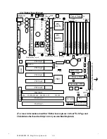
TYAN S1686D
TAHOE2I ATX
Pentium II 233 through 300 MHz
440 FX PCI-ISA System Board
Revision 1.0