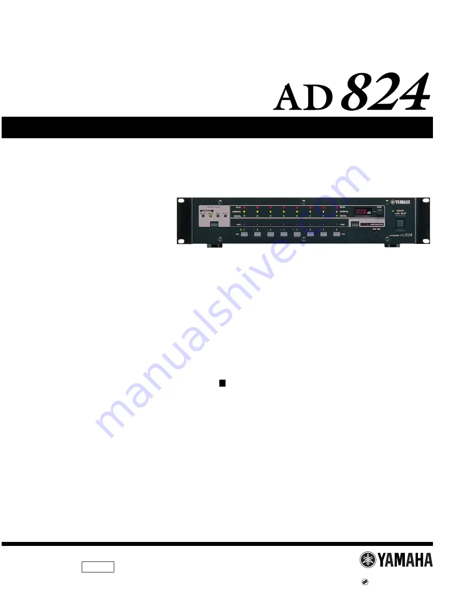
background image

SERVICE MANUAL

PA 

011523

HAMAMATSU, JAPAN

1.45K-9731 K 

Printed in Japan  '00.07

CONTENTS

SPECIFICATIONS ···································································· 3
PANEL LAYOUT ······································································· 5
CIRCUIT BOARD LAYOUT ······················································ 6
DIMENTIONS ··········································································· 8
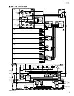
BLOCK DIAGRAM ···································································· 9
DISASSEMBLY PROCEDURE··············································· 10
LSI PIN DESCRIPTION ·························································· 14
IC BLOCK DIAGRAM ····························································· 16
CIRCUIT BOARDS ································································· 19
INSPECTION ·········································································· 36
TEST PROGRAM ··································································· 39
FLASH ROM UPGRADE ························································ 43
ERROR MESSAGES ······························································ 45
PARTS LIST
OVERALL CIRCUIT DIAGRAM

AD CONVERTER

200006**-150000

This document is printed on chlorine free (ECF) paper with soy ink.

Summary of Contents for AD824

Page 1: ... BOARD LAYOUT 6 DIMENTIONS 8 BLOCK DIAGRAM 9 DISASSEMBLY PROCEDURE 10 LSI PIN DESCRIPTION 14 IC BLOCK DIAGRAM 16 CIRCUIT BOARDS 19 INSPECTION 36 TEST PROGRAM 39 FLASH ROM UPGRADE 43 ERROR MESSAGES 45 PARTS LIST OVERALL CIRCUIT DIAGRAM AD CONVERTER 200006 150000 This document is printed on chlorine free ECF paper with soy ink ...

Page 2: ...tice or obligation to retrofit Should any discrepancy appear to exist please contact the distributor s Service Division WARNING Static discharges can destroy expensive components Discharge any static electricity your body may have accumulated by grounding yourself to the ground bus in the unit heavy gauge black wires connect to this bus IMPORTANT Turn the unit OFF during disassembly and parts repl...

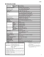
Page 3: ...humidity Power cord length Supplied accessories Options 39 69 50 88 kHz 41 013 50 88 kHz 24 bit linear 128 times oversampling 1 5 1 dB 20 Hz 20 kHz GAIN 10 dB 3 1 dB 20 Hz 20 kHz GAIN 62 dB 110 dB typical GAIN 10 dB 1 dB 1 kHz GAIN 62 dB to 10 dB 0 1 4 dB output 20 Hz 20 kHz GAIN 62 dB 0 05 full scale output 1 kHz GAIN 62 dB 0 05 4 dB output 20 Hz 20 kHz GAIN 10 dB 0 01 full scale output 1 kHz GAI...

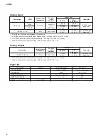
Page 4: ... dB 10 dB 62 dB 615 µV 10 dB 2 45 V 10 dB 2 45 V 48 dB 3 08 mV 24 dB 12 28 V 24 dB 12 28 V XLR 3 31 type balanced 2 TRS phone jack balanced 3 1 TRS phone jacks are electronically balanced tip hot ring cold sleeve ground Where dB represents a specific voltage 0 dB is referenced to 0 775 V rms Analog Output Connection Actual Source Impedance For Use with Nominal Connector Output Level Nominal Max be...

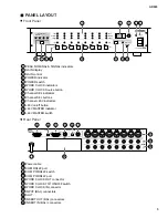
Page 5: ...PEAK NOMINAL SIGNAL indicators 2 GAIN display 3 GAIN control 4 POWER indicator 5 POWER switch 6 WORD CLOCK indicators 7 WORD CLOCK Source button 8 Channel SEL indicators 9 Channel SEL buttons 10 Channel 48V indicators 11 48V on off button 12 48V MASTER indicator 13 48V MASTER switch 14 Power cable 15 16 COM RS422 port COM PC RS422 switch 17 COM PC RS422 port 18 WORD CLOCK OUT connector 19 WORD CLO...

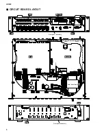
Page 6: ...D LAYOUT MAIN MYSL HA JK AD AC Rear panel assembly Front panel assembly Power transformer PN SW CN909 CN903 CN906 CN902 CN904 CN905 CN901 CN908 CN907 CN101 CN201 CN002 CN001 CN961 CN960 CN962 CN963 CN052 CN053 CN051 CN054 ...

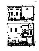
Page 7: ...AD824 7 JK AD CN103 AD CN104 AD CN204 CN203 CN202 CN102 CN005 CN004 CN002 CN001 CN003 CN004 CN001 CN003 MYSL AC DC PN SW CN002 CN008 CN010 CN011 CN007 CN006 CN005 CN009 ...

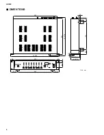
Page 8: ...AD824 8 DIMENTIONS 67 5 67 5 345 35 35 410 430 13 88 H 97 5 30 30 48 33 274 10 8 45 17 355 D 377 6 W 480 Unit mm ...

Page 9: ...CN051b CN051a CN901 OUT3 4 OUT7 8 OUT1 2 OUT5 6 CN904 CN905 CN961 SWA SWA SWB ECA ECB 48 CN960 CN902 CN053 CN902 CN053 CN054 BUFF IC933 MUTE PC RS422 RS422 IC901 COM B SLOT SELECT IC903 INT EXT SELECT IC913 SELECT IC910 D FF IC907 INT 48kHz X902 INT 44 1kHz X901 WORD CLOCK SELECT IC921 PLL TIMING GEN IC922 CN903 CN909 PC ON OFF RS422 EXT DIRIN XI CN907 CN908 RESET SLOT SLOT D FF D FF RES EXTAL 44 ...

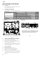
Page 10: ...he HA circuit board See procedure 2 4 3 Remove the JK circuit board See procedure 3 4 4 Remove the six 6 screws marked 330 the two 2 screws marked 350 and the two 2 screws marked 370 The AD circuit board can then be removed Fig 2 and Fig 3 AD824 10 DISASSEMBLY PROCEDURE 1 Top Cover 1 1 Remove the fourteen 14 screws marked 500 The top cover can then be removed Fig 1 2 Circuit Boards and Units Remov...

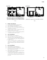
Page 11: ...then be removed Fig 5 6 AC Circuit Board 6 1 Remove the top cover See procedure 1 6 2 Remove the MAIN circuit board See procedure 2 6 3 Remove the three 3 screws marked 50A and the two 2 screws marked 110A The AC circuit board can then be removed Fig 6 The fuse is not a part of the AC circuit Board When you replace the AC circuit board you should remove the fuse from the board and put it back into...

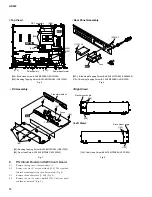
Page 12: ...e 1 8 2 Remove the six 6 screws marked 140 The right and left rack mount angles can then be removed Fig 8 8 3 Remove the knob marked 110B Fig 9 8 4 Remove the six 6 screws marked 80 The front panel can then be removed Fig 9 AC 250 Bind Head Screw 4 0X8 MFZN2BL EG340360 260 Bonding Tapping Screw B 3 0X8 MFZN2BL VN413300 Fig 5 Top View DC assembly OPT assembly MYSL Power transformer 190 260 260 210 ...

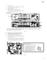
Page 13: ...50B 30 80 80 110B 90 Front panel 30 AD824 13 8 5 PN Circuit Board Remove the four 4 screws marked 30 The PN circuit board can then be removed Fig 9 8 6 SW Circuit Board Remove the PSW knob marked 90 Fig 9 Remove the two 2 screws marked 50B The SW circuit board can then be removed Fig 9 9 Replacement of the Lithium Battery 9 1 Remove the top cover See procedure 1 9 2 Remove the MAIN circuit board S...

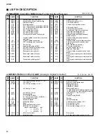
Page 14: ...status output method selection External synchronous auxiliary input word clock EIAJ AES EBU data input PLL word clock output Logic section power 5 V Data error flag output Channel status emphasis control code output 3 wire type microcomputer interface data output 3 wire type microcomputer interface clock input 3 wire type microcomputer interface load input YM3436DK XG948E0 DIR2 Digital Format Inte...

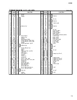
Page 15: ...ct Interrupt request Data transmission Data reception Interrupt request Port A Data transmission Port A Data reception Data bus Ground Data bus 57 58 59 60 61 62 63 64 65 66 67 68 69 70 71 72 73 74 75 76 77 78 79 80 81 82 83 84 85 86 87 88 89 90 91 92 93 94 95 96 97 98 99 100 101 102 103 104 105 106 107 108 109 110 111 112 D11 D10 D9 D8 VSS D7 D6 D5 VCC D4 D3 D2 D1 D0 VSS XTAL MD3 EXTAL MD2 NMI VC...

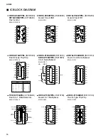
Page 16: ...4B INPUTS OUTPUTS PR CLR CLK D Q Q L H H L H Q O H L H H L Q O X X X H L X X X X f f L H L L H H H L H L H H H 1 2 3 4 5 6 7 1CLR 1D 1CK 1PR 1Q 1Q GND 14 13 12 11 10 9 8 VCC 2CLR CLR 2D D 2CK CK 2PR PR 2Q 2Q Q Q CLR D CK PR Q Q IC917 IC009 1 2 3 4 5 6 7 A A Select Enable Output Output B B C C G2A G2A G2B G2B G1 G1 Y7 Y7 Y5 Y4 Y3 Y2 Y1 Y0 Y6 16 15 14 13 12 11 10 Vcc YO Y1 Y2 Y3 Y4 Y5 8 GND 9 Y6 1 2...

Page 17: ... 8Q 8D 7D 7Q 6Q 6D 5D 5Q CLOCK 1 20 2 19 3 18 4 17 5 16 6 15 7 14 8 13 9 12 10 11 Q D CK CL D Q CK CL Q D CK CL D Q CK CL D Q CK CL Q D CK CL D Q CK CL Q D CK CL Vcc 2F 2E 2A 2Y GND 1Y 1 2 3 4 5 6 7 8 9 10 11 12 13 14 15 16 2C 2B 2D 1A 1B 1C 1D 1E 1F IC901 904 906 908 909 932 934 IC008 IC008 IC925 928 IC001 006 1A 1B 2R 2S 2A 2B 2Y GND 1 16 2 15 3 14 4 13 5 12 6 11 7 10 8 9 Vcc 1S 1R 1Y 3A 3S 3R 3...

Page 18: ...JK 1 2 3 4 V 8 7 6 5 Output A V Non Inverting Input A DC Voltage Supply DC Voltage Supply Output B Inverting Input B Non Inverting Input B Inverting Input A IC918 IC103 104 203 204 303 304 403 404 503 504 603 604 703 704 803 804 IC101 201 301 401 501 601 701 801 IC101 301 501 701 IC101 201 301 401 501 601 701 801 ...

Page 19: ...31C0 19 AC Circuit Board H W B XY032C0 19 AD Circuit Board XY028A0 28 DC Circuit Board J U V XY031C0 34 DC Circuit Board H W B XY032C0 35 HA Circuit Board XY029A0 24 JK Circuit Board XY028A0 29 MAIN Circuit Board XY030A0 20 MYSL Circuit Board XY030A0 21 PN Circuit Board XY027B0 32 SW Circuit Board J U V XY031C0 19 SW Circuit Board H W B XY032C0 19 Note See parts list for details of circuit board c...

Page 20: ...to AD CN003 MAIN Circuit Board A A 3NA V579130 to HA CN002 to MYSL CN054 to PN CN960 to PN CN961 to MYSL CN053 from DC CN010 AD824 20 ...

Page 21: ...103600 Battery holder for VN103500 Notice for back up battery removal Push the battery as shown in figure then the battery will pop up Druk de batterij naar beneden zoals aangeven in de tekening de batterij springt dan naar voren Battery Battery holder COM from DC CN008 from MAIN CN901 AD824 21 Component side Component side ...

Page 22: ...MAIN Circuit Board B B 3NA V579130 AD824 22 ...

Page 23: ...E B B MAIN MYSL 3NA V579130 MYSL Circuit Board AD824 23 Pattern side Pattern side ...

Page 24: ...3NA V579110 INPUT BAL 1 2 3 4 5 6 7 8 1 HA Circuit Board C C AD824 24 ...

Page 25: ...AD824 25 3NA V579110 to MAIN CN903 1 C C to JK CN202 to JK CN102 to DC CN007 Component side ...

Page 26: ...HA Circuit Board 3NA V579110 1 D D AD824 26 ...

Page 27: ...3NA V579110 1 D D AD824 27 Pattern side ...

Page 28: ...AD824 28 3NA V579120 AD Circuit Board E E INSERT IN BAL to MAIN CN909 1 2 3 4 5 6 7 8 to JK CN203 to JK CN103 ...

Page 29: ...AD824 29 JK Circuit Board E E AD JK 3NA V579120 INSERT OUT BAL to DC CN011 1 2 3 4 5 6 7 8 from HA CN201 to AD CN204 from HA CN101 to AD CN104 to PN CN962 Component side Component side ...

Page 30: ...AD824 30 AD Circuit Board 3NA V579120 F F ...

Page 31: ...AD824 31 JK Circuit Board F F AD JK 3NA V579120 Pattern side Pattern side ...

Page 32: ...3NA V579100 1 PN Circuit Board G G G G from DC CN009 to MAIN CN905 from AD CN002 to MAIN CN904 AD824 32 Component side ...

Page 33: ...PN Circuit Board 3NA V579100 1 H H H H AD824 33 Pattern side ...

Page 34: ...to MYSL CN052 DC Circuit Board J U V 3NA V579140 1 I I I I Power transformer Power transformer to MAIN CN906 to AD CN001 to PN CN963 to HA CN001 AD824 34 Component side ...

Page 35: ...DC Circuit Board H W B 3NA V579150 1 J J J J to MYSL CN052 Power transformer Power transformer to MAIN CN906 to AD CN001 to PN CN963 to HA CN001 AD824 35 Component side ...

Page 36: ...h The system will start up and initialize 2 Inspections 2 1 INPUT1 to 8CH 1 Gain 2 f characteristics Conditions Permissible range uses 1 kHz as a reference 3 Distortion ratio 4 Residual noise Conditions Input 1 to 8 channels shorted using 150 ohms AD824 36 INSPECTION Input frequency Input level GAIN Specified output level DA824 Permissible range 1 kHz 10 dB 4 dB 2 dB 8 dB 14 dB 20 dB 26 dB 32 dB 3...

Page 37: ...ecified level to AD824 input 1 to 8 AD824 can also have simultaneous input of channels 1 to 8 Visually confirm the on and off of the peak nominal and signal LEDs 1 On Lit 2 Off Not lit 2 5 Jitter measurement 1 INTERNAL 44 1 kHz 48 kHz Insert MY8 AE card into the slot and connect to DSA1 via the D sub cannon converter box Set AD824 word clock settings to 44 1 kHz and 48 kHz AD824 37 LED level Input...

Page 38: ...1 kHz 10 Set the oscillator to 39 69 kHz Make the same input as 2 6 1 and confirm that the same output level is attained Or conduct a listening test for one minute to check that there is no noise 3 Sound Perform a listening test to confirm the following items INPUT1 to 8 4 Initialization While pressing the SEL4 key and 48V key turn on the power switch The system will start up and initialize Others...

Page 39: ...l inspection 9 GAIN encoder connection check manual inspection 10 COM PC RS422 terminal check visual 11 Initializes memory Execute the test program after loading DA824DIAG V1 00 program The test program cannot be loaded while the turning jig is attached to COM RS422 terminal CN908 2 Test procedure execution program Connect the PC and COM RS422 terminals CN903 with a Dsub 9 pin serial cross cable a...

Page 40: ...rminals CN903 connection check 6 WORD CLOCK IN OUT terminal connection check During the program execution d will appear on the 7segLED The condition will also appear on the terminal software as shown below If the inspection ends normally the following will appear on the terminal software d00 will also come on 7segLED If there is an error the error list will appear on the terminal software After E0...

Page 41: ...lts will be shown on the screen 5 WC BNC Displayed on the screen when the results of the word clock IN terminal JK901 and CPU connection are NG 6 COM B Displayed on the screen when the results of the COM RS422 terminals CN903 and CPU connection are NG 4 d01 LED inspection Select the test program number d01 with the gain encoder The LED inspection will be executed when the 48V key is pressed Or it ...

Page 42: ...e gain encoder When the 48V key is pressed the program version will be displayed on 7segLED for approximately one second 7 d09 Initializes memory Select the test program number d09 with the gain encoder When the 48V key is pressed memory initialization is executed Or it can also be executed by entering When this program number is executed the following will be displayed on the terminal software 8 ...

Page 43: ...AD824 V1 0 is used as the software When the folder is open three files are displayed on the screen LoadAD824 exe TimeStamp exe and 02rv2 dll The two files requiring an upgrade are LoadAD824 exe and 02rv2 dll 2 1 Start the software Click on LoadAD824 exe The program will start and the following screen will be displayed It is also possible to switch the PC COM terminal that is connected by the dialo...

Page 44: ... 4 Loading the program Click the Load switch and the program will start to load When completed the following message will be displayed 2 5 Others Click the Disconnect switch to reset the AD824 to the regular mode ...

Page 45: ...stic checks when it s turned on If a problem isdetected one of the following error codes appears briefly on the GAIN display Internal backup battery voltage low Internal memory data corrupt Internal backup battery voltage low and internal memory data corrupt ...

Page 46: ...opean model I Indonesian model J Japanese model M South African model O Chinese model Q South east Asia model T Taiwan model U U S A model V General export model 110 V W General export model 220 V N X General export model Y Export model Notes DESTINATION ABBREVIATIONS The numbers in QTY show quantities for each unit The parts with in PART NO are not available as spare parts The mark in the remarks...

Page 47: ...90 330 530 520 290 80 40 Rear panel assembly see page 5 150 270 540 310 320 300 50 380 350 340 360 200 210 205 160 170 30 60 250 240 370 430 480 490 230 25 35 70 80 33 34 32 140 130 120 190 120 180 110 10b 10c 10d 10a 10 220 260 DC assembly see page 6 Front panel assembly see page 4 ...

Page 48: ...80 180 190 200 200 205 210 220 230 240 250 260 270 290 300 310 320 330 340 350 360 370 380 390 400 420 430 440 445 450 460 470 480 490 500 REF NO V4067500 CB806590 VR138400 CB835590 VC362700 CB069250 CB095100 VC688800 EG340360 V4068400 VC688800 V4605100 VC688800 VC688800 V4705100 V6221000 VN413300 XY173A00 XY174A00 XY175B00 VC688800 V5610800 V5610900 CB817510 VC688800 V4093800 V5792200 EG340360 VN...

Page 49: ... Sub Chassis Circuit Board Bind Head Tapping Screw B Circuit Board Circuit Board Bonding Screw Front Panel Cover Oval Head Screw Power Switch Knob Escutcheon Power Switch Knob DESCRIPTION 10 20 30 40 40 50 60 70 80 90 100 110 REF NO V4067800 V5791000 EP600230 V5792500 V5792800 VS863000 V4067900 V4068900 VS153600 VL812900 VL813000 VM840900 PART NO PN 3 0X6 MFZN2BL SW SW 3 0X6 MFZN2BL 4 0X8 MFZN2BL ...

Page 50: ...20 30 30 30 40 40 60 80 90 100 110 F001 F001 REF NO V4068100 V5254600 V5254700 VS228900 VS229000 VS229100 VS229200 CB806850 CB811230 CB032840 V5792300 V5792600 VC688800 VC362700 CB069250 V5274400 VN413300 KB003570 KB003040 PART NO AD AD AD 2P 15A 3P 10A 3P 6A 3P 10A SR 6N3 4 SR 6N 4 SR 5N 4 AC AC A4 0X8 MFZN2BL FR25 15 12 1400L BK 1 3 0X8 MFZN2BL 2 00A JU 1 00A S AD824 J V561020 U V V561030 H W V5...

Page 51: ...5792700 VN413300 EL200020 KB003560 KB003060 KB003560 KB003060 KB003570 KB003070 KB003570 KB003070 KB003630 KB003240 KB003470 KB003010 PART NO DC DC 3 0X8 MFZN2BL SP 4 0X8 MFZN2Y 1 60A JU 1 60A S 1 60A JU 1 60A S 2 00A JU 2 00A S 2 00A JU 2 00A S 5 00A JU 5 00A S 500mA 250V JU 500mA S AD824 J U V H W B V406870 J U V H W B V406820 J U V H W B J U V H W B J U V H W B J U V H W B J U V H W B J U V H W...

Page 52: ...00 V5731700 V5724900 VA078900 V3311600 V5170300 VS589000 VS589000 UR659220 UR659220 UR639470 UR639470 VT947800 VT598700 UA355100 UA355100 VS589000 UR897100 UR858100 UR838100 VS589000 UR897470 LB932030 LB933030 LB933030 LB933040 LB932060 LB932050 VK025800 VK025700 VF728200 VK024900 VK025700 VB481900 VB481900 VT359600 VT359600 VN011300 VB845300 FZ006970 FZ006970 VP206500 VP206500 XD853A00 XD854A00 X...

Page 53: ...37 C138 C139 C140 REF NO XD631A00 VA078900 VA078900 BB069510 BB069510 VQ764500 VC749400 HF757220 HF756560 HF758100 VC743400 HF757100 HF757100 HF756220 VC750200 HF756220 HF757100 HF757100 VC330400 VC328600 HF756470 V3127000 VS150800 VM923000 VS150800 VS150800 VM923000 IA101590 VQ554100 VQ558500 VQ557800 V5791900 V5792000 V5274300 V5829300 V5829300 V5829200 V5829200 UB245100 UB245100 UU148100 UU1481...

Page 54: ...4 C405 C406 C416 C417 C418 420 C421 C422 C423 C427 C443 446 C501 C502 C503 C504 C505 C506 C516 C517 C518 REF NO UB044100 UB044100 UB044100 UB044100 UB051220 UB051220 UU148100 UU148100 UU167100 UU167100 UB052100 UB052100 UU167100 UB052220 UB052220 UA353220 UB044100 UB044100 UB044100 UB044100 UB051220 UB051220 UU148100 UU148100 UU167100 UU167100 UB052100 UB052100 UU167100 UB052220 UB052220 UA353220 ...

Page 55: ...1 C732 C733 C734 C735 C736 C737 C738 C739 C740 C743 746 C801 C802 C803 C804 C805 C806 C816 C817 C818 REF NO UB052100 UU167100 UB052220 UB052220 UA353220 UB245100 UU167100 UB245220 UB245100 UU167100 UB245220 UB245100 UU167100 UB245100 UU147220 UU147220 UB044100 UB044100 UB044100 UB044100 UB051220 UB051220 UU148100 UU148100 UU167100 UU167100 UB052100 UB052100 UU167100 UB052220 UB052220 UA353220 UB04...

Page 56: ...44A00 XJ553A00 XJ553A00 XV065A00 XP844A00 XJ553A00 XJ553A00 XP844A00 XJ553A00 XJ553A00 XV065A00 XP844A00 XJ553A00 XJ553A00 XP844A00 XJ553A00 XJ553A00 XV065A00 XP844A00 XJ553A00 XJ553A00 LB301920 LB301920 LB301920 LB301920 PART NO SL 100P 50V J 10 00 50 0V SL 220P 50V J SL 220P 50V J 2200P 50V J F 0 010 50V Z F 0 010 50V Z 51048 13P TE 52147 16P TE 51048 16P TE 52147 7P TE 51048 7P TE 51048 12P TE ...

Page 57: ...920 LB301920 LB301920 LB301920 VS740100 VS740100 RD255100 RD255100 RD258100 VC328900 VC328900 VC328800 VC329700 VC329700 VC329600 VC329600 HF754750 HF754750 RD258100 RD258100 HF755100 HF758100 HF758100 VC328800 VC328800 VC328100 VC328100 HF754390 HF758100 VC329200 VC327100 VC327200 VC327200 HF754470 HF754470 VC327400 VC328900 VC327400 HF754390 RD258100 VC328900 VC328900 VC328800 VC329700 VC329700 ...

Page 58: ...32 R433 R434 R435 R436 R437 R438 R439 R440 R441 R445 R501 R502 504 R505 R506 R507 REF NO VC327200 VC327200 HF754470 HF754470 HF754390 RD258100 VC328900 VC328900 VC328800 VC329700 VC329700 VC329600 VC329600 HF754750 HF754750 RD258100 RD258100 HF755100 HF758100 HF758100 VC328800 VC328800 VC328100 VC328100 HF754390 HF758100 VC329200 VC327100 VC327200 VC327200 HF754470 HF754470 VC327400 VC328900 VC327...

Page 59: ...2 704 R705 R706 R707 R708 R709 R710 R711 R712 R713 R727 R728 R729 R730 R731 REF NO VC329600 VC329600 HF754750 HF754750 RD258100 RD258100 HF755100 HF758100 HF758100 VC328800 VC328800 VC328100 VC328100 HF754390 HF758100 VC329200 VC327100 VC327200 VC327200 HF754470 HF754470 VC327400 VC328900 VC327400 HF754390 RD258100 VC328900 VC328900 VC328800 VC329700 VC329700 VC329600 VC329600 HF754750 HF754750 RD...

Page 60: ...Cap Monolithic Ceramic Cap Electrolytic Cap Electrolytic Cap KL Electrolytic Cap KL Monolithic Ceramic Cap Monolithic Ceramic Cap Monolithic Ceramic Cap Monolithic Ceramic Cap Electrolytic Cap Monolithic Ceramic Cap Monolithic Ceramic Cap Monolithic Ceramic Cap DESCRIPTION R732 R733 R734 R735 R736 R737 R738 R739 R740 R741 R742 R743 R744 R745 R801 R802 804 R805 R806 R807 R808 R809 R810 R811 R812 R8...

Page 61: ...ic Cap Monolithic Ceramic Cap Monolithic Ceramic Cap Monolithic Ceramic Cap Electrolytic Cap Monolithic Ceramic Cap Monolithic Ceramic Cap Monolithic Ceramic Cap Electrolytic Cap Monolithic Ceramic Cap Electrolytic Cap Monolithic Ceramic Cap Monolithic Ceramic Cap Monolithic Ceramic Cap Monolithic Ceramic Cap Monolithic Ceramic Cap Monolithic Ceramic Cap Electrolytic Cap Electrolytic Cap KL Electr...

Page 62: ...p KL Electrolytic Cap KL Monolithic Ceramic Cap Monolithic Ceramic Cap Monolithic Ceramic Cap Monolithic Ceramic Cap Electrolytic Cap Monolithic Ceramic Cap Monolithic Ceramic Cap Monolithic Ceramic Cap Monolithic Ceramic Cap Monolithic Ceramic Cap Electrolytic Cap Monolithic Ceramic Cap Monolithic Ceramic Cap Monolithic Ceramic Cap Electrolytic Cap Monolithic Ceramic Cap Electrolytic Cap Monolith...

Page 63: ...23 C824 C825 C828 C829 C841 C842 CN001 CN002 CN101 CN201 D101 103 D201 203 D301 303 D401 403 REF NO UB044100 UB051220 UB051220 UB245100 UB245100 UR877470 VJ097400 VJ097400 UB052220 UB052220 UB013100 UB013100 UR819100 UB051100 UB052220 UB051100 UB044100 UB044100 UU148100 UB052100 UB051330 UB052100 UU147470 UB044100 UU148100 UB044100 UB044100 UB051220 UB051220 UB245100 UB245100 UB245100 UR877470 VJ0...

Page 64: ... XC458A00 XJ553A00 XY879A00 XC458A00 VT838100 VT838100 VT838100 VT838100 VT838100 VT838100 VT838100 VT838100 VS740100 VV556400 VV556400 IC224030 IC224030 VV556400 VV556400 PART NO D1F60 D1F60 D1F60 D1F60 D1F60 D1F60 D1F60 D1F60 LS MT Y223NB LS MT Y223NB LS MT B271KB LS MT B271KB LS MT B271KB LS MT B271KB LS MT B271KB LS MT B271KB LS MT B271KB LS MT B271KB LS MT B271KB LS MT B271KB LS MT B271KB LS ...

Page 65: ...24030 IC224030 VV556400 VV556400 IC224030 IC224030 VV556400 VV556400 IC224030 IC224030 VV556400 VV556400 IC224030 IC224030 VV556400 VV556400 IC224030 IC224030 VV556400 VV556400 IC224030 IC224030 RD255100 VC328400 VC328400 VC326000 VC328000 VC327100 VC327100 HF754100 HF754100 VC330400 VC330400 HF754100 HF754100 VC327200 VC327200 VC323600 VC327600 VC328800 VC328600 VC328600 VC328800 VC328000 VC32800...

Page 66: ...Metal Film Resistor Metal Film Resistor Metal Film Resistor Metal Film Resistor DESCRIPTION REF NO HF754100 VC330400 VC330400 HF754100 HF754100 VC327200 VC327200 VC323600 VC327600 VC328800 VC328600 VC328600 VC328800 VC328000 VC328000 HF754390 VC327400 VC328600 VC328600 VC328000 VC330000 HF755100 HF754390 HF758100 HF758100 HF757100 HF757100 HV755390 HF758100 VC328400 VC328400 VC326000 VC328000 VC32...

Page 67: ... R525 R526 R527 R528 R529 R530 R531 R532 R533 R534 R535 R545 547 R548 R549 R601 R602 R605 REF NO VC327100 HF754100 HF754100 VC330400 VC330400 HF754100 HF754100 VC327200 VC327200 VC323600 VC327600 VC328800 VC328600 VC328600 VC328800 VC328000 VC328000 HF754390 VC327400 VC328600 VC328600 VC328000 VC330000 HF755100 HF754390 HF758100 HF758100 HF757100 HF757100 HV755390 HF758100 VC328400 VC328400 VC3260...

Page 68: ... R723 R724 R725 R726 R727 R728 R729 R730 R731 R732 R733 R734 R735 R745 747 R748 R749 R801 REF NO VC328000 VC327100 VC327100 HF754100 HF754100 VC330400 VC330400 HF754100 HF754100 VC327200 VC327200 VC323600 VC327600 VC328800 VC328600 VC328600 VC328800 VC328000 VC328000 HF754390 VC327400 VC328600 VC328600 VC328000 VC330000 HF755100 HF754390 HF758100 HF758100 HF757100 HF757100 HV755390 HF758100 VC3284...

Page 69: ...C328400 VC326000 VC328000 VC327100 VC327100 HF754100 HF754100 VC330400 VC330400 HF754100 HF754100 VC327200 VC327200 VC323600 VC327600 VC328800 VC328600 VC328600 VC328800 VC328000 VC328000 HF754390 VC327400 VC328600 VC328600 VC328000 VC330000 HF755100 HF754390 HF758100 HF758100 HF757100 HF757100 HV755390 HF758100 VU685600 VU685600 VU685600 VU685600 VU685600 VU685600 VU685600 VU685600 VU685600 VU685...

Page 70: ...Q048500 VN520900 VK025800 VK025100 VI878300 VU196300 VU196300 VJ861600 VT332900 VT332900 VQ761400 FZ006970 FZ006970 VQ761400 IS024500 XN976A00 XU073A00 IS024500 IS024500 IS007400 IS024500 IS024500 XY309A00 XV731A00 IS000800 XY309A00 IS000400 IS013910 XI686A00 IS013810 XN797A00 IS007400 XY102A00 XG948E00 XG948E00 XV411A00 XV411A00 IS027300 IS003200 PART NO B 470P 50V K F 0 100 25V Z F 0 100 25V Z S...

Page 71: ...15700 VI552200 VI552200 VI474400 VS740100 VS740100 GE300610 VS740100 VS740100 GE300610 GE300610 VS740100 VS740100 RD254750 RD254470 RD257100 RD257100 RD254100 RD254100 RD255470 RD255470 RD254100 RD254100 RD257100 RD256470 RD256470 RD256100 RD257100 RD256300 RD255200 RD259470 RD258100 RD258100 RD255470 RD257100 RD259100 RD256200 RD256200 VI195100 VI195100 RD256220 RD253470 RD255200 RD256150 RD25000...

Page 72: ...301 REF NO UB245100 UB245100 UB044100 UB044100 UF047100 UF047100 UB245100 UB245100 UF047100 UF047100 UB245100 UB245100 UB044100 UB044100 UF047100 UF047100 UB245100 UB245100 UF047100 UF047100 UB245100 UB245100 UB044100 UB044100 UF047100 UF047100 UB245100 UB245100 UF047100 UF047100 UB245100 UB245100 UB044100 UB044100 UF047100 UF047100 UB245100 UB245100 UB245100 UB245100 UF047330 UF047330 UB245100 UB...

Page 73: ...10400 VV310400 VV311300 VV310400 VV356300 RD257100 RD257470 RD257470 RD256220 RD256220 RD257470 RD257470 RD255390 RD255390 VV324300 VV310400 VV310400 VV311300 VV310400 VV356300 RD257100 RD257470 RD257470 RD256220 RD256220 RD257470 RD257470 RD255390 RD255390 VV324300 VV310400 VV310400 VV311300 VV310400 VV356300 RD257100 PART NO NJM2068MD T1 NJM2068MD T1 SLZ 135B 08 T1 RE SLZ 435B 08 T1 YE SLZ 235B ...

Page 74: ...13 R514 516 R517 519 R601 R602 R603 R604 R605 R606 R607 R608 610 R611 613 R614 616 R617 619 R701 R702 R703 R704 R705 R706 R707 R708 710 R711 713 R714 716 R717 719 R801 R802 REF NO RD257470 RD257470 RD256220 RD256220 RD257470 RD257470 RD255390 RD255390 VV324300 VV310400 VV310400 VV311300 VV310400 VV356300 RD257100 RD257470 RD257470 RD256220 RD256220 RD257470 RD257470 RD255390 RD255390 VV324300 VV31...

Page 75: ...255390 RD255390 RD256820 RD256330 RD256180 RD256120 RD256820 RD256330 RD256180 RD256120 RD254330 RD254330 RD254470 RD254470 RD258100 V5537600 VV056000 VV056000 VQ248500 VQ248400 VV556400 VV556400 VV556500 VV556500 VV556400 VV556400 VV556500 VV556500 VV556400 VV556400 VV556500 VV556500 VV556400 VV556400 VV556500 VV556500 VV556400 VV556400 VV556500 VV556500 VV556400 VV556400 VV556500 VV556500 VV5564...

Page 76: ...00 VS229200 KB003570 KB003040 KB003560 KB003060 KB003560 KB003060 KB003570 KB003070 KB003570 KB003070 KB003630 KB003240 KB003470 KB003010 PART NO CEE A CR2032 2P 15A 3P 10A 3P 6A 3P 10A 2 00A JU 1 00A S 1 60A JU 1 60A S 1 60A JU 1 60A S 2 00A JU 2 00A S 2 00A JU 2 00A S 5 00A JU 5 00A S 500mA 250V JU 500mA S H W B J U V H W B J U V H W B J U V H W B J U V H W B J U V H W B J U V H W B J U V H W B ...

Page 77: ... details of circuit board component parts Mylar Capacitor not installed BUFFER AND INVERTER OP AMP SYSTEM RESET D FF INVERTER SRAM 256K FLASH ROM 8M SRAM 256K CPU BUFFER BUFFER BUFFER to DC CN008 WORD CLOCK OUT to DC CN010 to PN CN961 to PN CN960 to HA CN002 to AD CN003 D FF D FF DECODER DECODER D FF BUFFER BUFFER BUFFER LINE DRIVER DIR2 DATA SELECTOR DATA SELECTOR D FF LINE RECEIVER DIR2 LINE DRE...

Page 78: ...e parts list for details of circuit board component parts Mylar Capacitor Electrolytic Cap not installed Metal Film Resistor to HA CN201 to HA CN101 to PN CN962 to DC CN011 to MAIN CN909 INSERT OUT BAL INSERT IN BAL OP AMP OP AMP OP AMP OP AMP DAC BUFFER INVERTER DAC DAC DAC OP AMP OP AMP OP AMP OP AMP OP AMP OP AMP OP AMP OP AMP OP AMP OP AMP OP AMP OP AMP OP AMP OP AMP OP AMP OP AMP OP AMP OP AM...

Page 79: ... D FF D FF D FF D FF D FF D FF OP AMP OP AMP OP AMP OP AMP OP AMP MULTIPLEXER MULTIPLEXER MULTIPLEXER MULTIPLEXER OP AMP MULTIPLEXER OP AMP OP AMP OP AMP OP AMP OP AMP OP AMP MULTIPLEXER OP AMP OP AMP MULTIPLEXER OP AMP OP AMP to JK CN102 to MAIN CN903 to DC CN007 to JK CN202 Note See parts list for details of circuit board component parts Electrolytic Cap Metal Film Resistor Flame Proof C Resisto...

Page 80: ...200V S1WB A 60 VB845300 DIODE STACK 1 0A 11ES4 VB481900 DIODE 1 2 1 ANODE 2 CATHODE 1 2 1 ANODE 2 CATHODE D1F60 VS201100 DIODE 1 ANODE 2 CATHODE 2 1 Note See parts list for details of circuit board component parts TO SERVICE PERSONNEL Critical Components Infomation Components having special characteristics are marked and must be replaced with parts having specifications equel to those originally i...

Reviews: