background image

DVD-C996/DV-C6280

DVD-C996

DV-C6280

1 0 0 7 2 8

SERVICE MANUAL

DVD PLAYER

This manual has been provided for the use of authorized YAMAHA Retailers and their service personnel.
It has been assumed that basic service procedures inherent to the industry, and more specifically YAMAHA Products, are
already known and understood by the users, and have therefore not been restated.

WARNING:

Failure to follow appropriate service and safety procedures when servicing this product  may result in
personal injury, destruction of expensive components, and failure of the  product to perform as specified.
For these reasons, we advise all YAMAHA product owners that any service required should be performed
by an authorized YAMAHA Retailer or the appointed service representative.

IMPORTANT:

The presentation or sale of this manual to any individual or firm does not constitute authorization,  certifi-
cation  or  recognition  of  any  applicable  technical  capabilities,  or establish a principle-agent relationship
of any form.

The data provided is believed to be accurate and applicable to the unit(s) indicated on the cover.  The research, engineering,
and service departments of YAMAHA are continually striving  to improve YAMAHA products. Modifications are, therefore,
inevitable and specifications are subject to change without notice or obligation to retrofit. Should any discrepancy appear to
exist, please contact the distributor's Service Division.

WARNING:

Static discharges can destroy expensive components. Discharge any static electricity your body may have
accumulated by grounding yourself to the ground buss in the unit (heavy gauge black wires connect to this
buss).

IMPORTANT:

Turn the unit OFF during disassembly and part replacement. Recheck all work before you apply power to
the unit.

IMPORTANT NOTICE

DVD-C996

DV-C6280

SERVICE MANUAL

 CONTENTS

TO SERVICE PERSONNEL ......................................... 1
PREVENTION OF ELECTRO STATIC DISCHARGE (ESD) TO
ELECTRO STATICALLY SENSITIVE (ES) DEVICES ....................... 
3
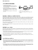
PRECAUTION, LASER DIODE 
.................................... 4
HANDLING PRECAUTIONS FOR TRAVERSE DECK 
......... 4
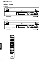
FRONT PANELS 
........................................................... 5
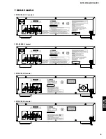
REAR PANELS 
......................................................... 6–7
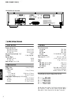
SPECIFICATIONS 
......................................................... 7
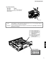
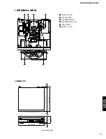
INTERNAL VIEW 
.......................................................... 8
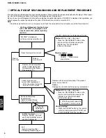
OPTICAL PICKUP SELF-DIAGNOSIS AND
REPLACEMENT PROCEDURE ................................... 
9
SELF-DIAGNOSIS FUNCTION AND SERVICE
MODES .................................................................. 
10–11
SERVICE PRECAUTIONS 
.......................................... 11

SERVICE TOOLS AND EQUIPMENT ........................ 12
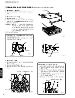
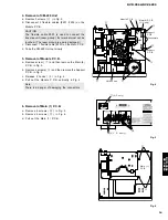
DISASSEMBLY PROCEDURES 
.......................... 13–16
ASSEMBLING AND DISASSEMBLING THE OPTICAL
PICKUP ................................................................... 17–22
ADJUSTMENT ....................................................... 23–26
SPECIAL FUNCTIONS FOR MAINTENANCE ..... 
27–27
IC DATA 
................................................................ 29–32
DISPLAY DATA 
.......................................................... 33
ABBREVIATIONS 
................................................. 34–35
PRINTED CIRCUIT BOARD 
................................. 36–47
SCHEMATIC DIAGRAM 
....................................... 48–64
BLOCK DIAGRAM 
................................................ 65–69
REMOTE CONTROL TRANSMITTER ........................ 
70
PARTS LIST 
.......................................................... 71–88

Summary of Contents for DVD-C996

Page 1: ...ly striving to improve YAMAHA products Modifications are therefore inevitable and specifications are subject to change without notice or obligation to retrofit Should any discrepancy appear to exist p...

Page 2: ...y result in hazardous radiation exposure WARNING CHEMICAL CONTENT NOTICE The solder used in the production of this product contains LEAD In addition other electrical electronic and or plastic where ap...

Page 3: ...Max 1 0mW Continuous Output value determined by 21 CFR CHAPTER1 SUBCHAPTER J VARO AVATTAESSA JA SUOJALUKITUS OHITETTAESSA OLET ALTTIINA N KYM TT M LLE LASER S TEILYLLE L KATSO S TEESEEN VARNING OSYNLI...

Page 4: ...plying power to the unit under test 2 After removing an electrical assembly equipped with ES devices place the assembly on a conductive surface such as aluminum foil to prevent electrostatic charge bu...

Page 5: ...tical pickup 1 Do not subject the optical pickup to static electricity as it is extremely sensitive to electrical shock 2 To prevent the breakdown of the laser diode an antistatic shorting bridge is s...

Page 6: ...DVD C996 DV C6280 DVD C996 DV C6280 FRONT PANELS DVD C996 DV C6280 5...

Page 7: ...DVD C996 DV C6280 DVD C996 DV C6280 REAR PANELS DVD C996 U C models DV C6280 U model DVD C996 R model 240V 120V 110V 220V DVD C996 A model 6...

Page 8: ...oltage 1 kHz 0 dB 2 0 V VIDEO SECTION VIDEO output 1 Vp p 75 ohms S VIDEO output Y output 1 Vp p 75 ohms C output U C R models 0 286 Vp p 75 ohms A B G models 0 3 Vp p 75 ohms COMPONENT VIDEO output U...

Page 9: ...DV C6280 8 INTERNAL VIEW e r w t y q 435 17 1 8 16 5 8 100 3 15 16 116 4 9 16 3 1 8 6 1 4 395 15 9 16 404 15 7 8 DIMENSION Unit mm inch q MAIN 3 P C B w CM 220 UNIT e CLAMPER ASS Y r DVD MODULE P C B...

Page 10: ...alue into the unit if it is 45 or less Check the laser drive current Value is more than 55 Value is 55 or less Initialize the player End Refer to Handling After Completing Repairs page 11 Use the tilt...

Page 11: ...ptical Pickup Self Diagnosis and Replacement in page 9 Procedure Refer to Initializing the DVD Player in page 11 0 5 7 6 9 The service mode can be activated by pressing various button combinations on...

Page 12: ...the power turned on 1 Press the OPEN CLOSE button to close the tray 2 Press the POWER button to turn off the power 3 Disconnect the power plug from the outlet 2 1 Method Do not disconnect the power pl...

Page 13: ...sc to make optical adjustments 4 If adjustment is done using a warped disc the adjustment will be incorrect and some discs will not be playable DVDT S15 AAX07320 or DVDT S01 TX946080 JZS0100 TX946380...

Page 14: ...the table according to the following procedure 1 Slide the Lever so that the Gear RT becomes free Fig B 2 With the mark on the Gear RT aligned with the same mark on the Tray lock it with the Lever Fig...

Page 15: ...out slowly 5 Removal of Module P C B a Remove screw u and then remove the Main 6 P C B in Fig 5 b Remove 4 screws i and then remove the Support P C B in Fig 4 c Release 2 hooks o in Fig 4 d Pull out...

Page 16: ...Ass y out slowly Fig 8 Fig 7 9 Removal of Traverse Unit a Remove 3 screws 4 in Fig 8 Note Be sure to take static electricity countermeasures before disconnecting the flexible cable Refer to page 18 St...

Page 17: ...cable 22 pin AAX16610 JGS0116 CAUTION a As the grounding becomes loose when the Main P C B is removed from the chassis ground the board to the chassis b Do not allow anything like cloth insulating ma...

Page 18: ...and installation the terminals of the laser diode are short circuited After replacing the parts use the proper procedure to return the laser diode to its original condition Refer to page 22 Assembling...

Page 19: ...d then ground the sheet 3 1 Static Electricity Countermeasure Methods Solder the land in the flexible cable of the optical pickup Notes Be sure to do this before disconnecting the flexible cable of th...

Page 20: ...age 23 Optical Pickup Tilt Adjustment 4 Disassembling the Stepping Motor Unit 1 Disconnect the flexible cable 2 Remove the 2 screws Note Take care when handling the flexible cable bacause it can be br...

Page 21: ...arefully because the shape of the tip is easily deformed The sub shaft preload spring is not part of the optical pickup Before replacing the optical pickup remove the sub shaft preload spring for use...

Page 22: ...n page 9 Do this first after turning on the unit with NO disc and while the unit is cold within the first 3 minutes of power ON or the jitter reading will not be accurate for the new pickup head 9 Ass...

Page 23: ...gram Froil 946P part number TX946410 0 01g Screw lock Three Bond 1401C 0 02g part number TX946400 Screw lock Three Bond 1401C 0 02g part number TX946400 Screw lock Three Bond 1401C 0 02g part number T...

Page 24: ...see that JIT xxx is displayed Present jitter value Play test disc title 1 inner periphery Tangential adjustment screw Adjust to the minimum jitter value Do steps 3 5 from the bottom of the main unit...

Page 25: ...OWER button to turn off the power 3 Disconnect the power plug from the outlet Assemble the main unit Follow procedure for handling after repairs are completed End STEP6 Adjustment screws Screw lock 0...

Page 26: ...scope to the video output terminal and terminate at 75 ohms 2 Confirm that the luminance signal Y S level is 1000 mVp p 30 mV 2 Video Output Chrominance Signal Confirmation Do this confirmation after...

Page 27: ...ation value Screwdriver Oscilloscope 100mV div 10 usec div 525mVp p 11mV B A G Models 486mVp p 10mV U C R Models DVDT S15 AAX07320 or DVDT S01 TX946080 Purpose To maintain video signal output compatib...

Page 28: ...e 2 Test mode 2 DVD segment of FL turned on Not used Do not use this function as it is not for servicing No Player button Action 1 DISC 1 Changes the current table parameter to Braking when making a l...

Page 29: ...DVD C996 DV C6280 DVD C996 DV C6280 28 MEMO...

Page 30: ...input 29 TXD SBO0 P00 RXD SBI0 P01 SBT0 P02 SBO1 P03 SBI1 P04 SBT1 P05 DK BUZZER P06 VDD OSC2 OSC1 VSS XI XO MMOD VREF AN0 PA0 AN1 PA1 AN2 PA2 AN3 PA3 AN4 PA4 AN5 PA5 AN6 PA6 AN7 PA7 VREF P07 P95 SEG1...

Page 31: ...Grid signal output for FL display 56 P40 DGT8 6G Grid signal output for FL display 57 P77 SEG0 DGT7 7G Grid signal output for FL display 58 P76 SEG1 DGT6 8G Grid signal output for FL display 59 P75 S...

Page 32: ...SEG31 PB3 NC 89 PB2 SEG32 PB2 NC 90 PB1 SEG33 PB1 NC 91 PB0 SEG34 PB0 NC 92 PD7 SEG35 PD7 NC 93 PD6 SEG36 PD6 NC 94 PD5 SEG37 PD5 NC 95 PD4 SEG38 PD4 NC 96 PD3 SEG39 PD3 NC 97 PD2 SEG40 PD2 NC 98 PD1...

Page 33: ...or chroma video input for Bank B Logic input pin to select whether the outputs of CVOUT1 YOUTA and CVOUT2 YOUTB are from filtered or unfiltered CV sources Internally pulled low Logic input pin to sele...

Page 34: ...F2 Filament 2 NP No Pin 3 NC No Connection 4 P1 P15 Datum Line 5 1G 13G Grid PIN CONNECTION Pin No 1 2 3 4 5 6 7 8 9 10 11 12 13 14 15 16 17 18 19 20 21 22 23 24 25 26 27 28 29 30 Connection F1 F1 NP...

Page 35: ...UT D DACCK D A CONVERTER CLOCK DEEMP DEEMPHASIS BIT ON OFF DEMPH DEEMPHASIS SWITCHING DIG0 UP FL DIGIT OUTPUT DIN DATA INPUT DMSRCK DM SERIAL DATA READ CLOCK DMUTE DIGITAL MUTE CONTROL DO DROP OUT DOU...

Page 36: ...08 CP7009 C7015 R7001 72 109 75 76 50 100 26 51 1 2 5 144 37 73 108 1 36 C2041 C2034 C2038 C7020 C7021 C6203 C6204 C7022 C7023 C6212 C6207 R6301 C6302 RA6206 RA6205 RA6204 C2005 R5211CP5202 33 16 32 1...

Page 37: ...C4225 C7026 C7006 C7014 C3017 C3016 C6514 1 2 3 5 4 4 15 O I G 14 25 36 1 12 24 22 12 12 1 13 24 1 1 1 37 48 13 28 1 1 5 8 IC6303 IC4201 IC4211 IC6551 PS4201 IC6501 IC6301 C4204 L4211 RA7001 RA7002 LB...

Page 38: ...DOWN SCLOCK SEL1 GND YOUT GND VOUT GND NSW 5V 13V SDATA SCLOCK GND LOUT GND ROUT GND COUT FROM MODULE D 2 5V DGND D 5V MGND M 9V VGND Y VGND CB VGND NC 5 REM RS GND DGND 2 5V DGND A 5V AGND C VGND CR...

Page 39: ...B CLAMP UP DOWN SW FROM CM 4 CM 3 P C B LOADING SW FROM LOADING MOTOR FROM DISC CLAMP MOTOR FROM TRAY ROTATE MOTOR FROM CM 1 FROM CM 2 FROM CM 3 FROM MAIN 1 CM 4 P C B 1 10 1 10 Ref No Location D1 B3...

Page 40: ...6 5 0 1 0 0 7 6 5 4 1 3 U C only MAIN 2 P C B Surface Mount Device B G only U C only U C R A only A B G only R only A only 3 2 4 3 1 Point w XL352 V 2V div H 20 sec div DC range 1 1 probe Point e CH1...

Page 41: ...ce Mount Device U C only AV TO MAIN 1 TO MAIN 1 GND YOUT GND VOUT GND D 5 13V W286 204 W287 205 SDATA SCLOCK GND LOUT GND ROUT GND COUT MAIN 5 P C B Lead Type Device G B only FROM POWER CORD FROM MAIN...

Page 42: ...6 4 4 3 3 0 6 1 1 3 2 0 1 2 0 1 7 1 7 1 7 1 7 3 3 3 3 0 3 2 0 1 2 2 2 1 9 0 1 7 0 1 7 0 1 7 0 0 2 1 2 1 3 4 0 0 1 3 6 3 7 2 1 2 2 1 1 1 2 1 7 0 2 8 5 0 0 5 0 4 9 1 6 2 2 2 2 2 2 2 2 2 2 2 2 2 2 2 2 1...

Page 43: ...5 0 0 65 0 0 85 3 3 0 6 0 1 7 26 2 2 2 2 46 3 3 3 3 66 0 0 86 3 3 0 7 0 0 27 3 3 3 3 47 3 0 0 67 3 3 0 87 3 3 3 3 8 1 6 1 6 28 1 7 1 7 48 1 5 0 68 0 1 7 88 3 1 3 2 9 1 6 1 6 29 0 1 2 49 0 0 69 0 0 89...

Page 44: ...128 3 3 3 3 9 0 3 3 29 0 0 49 3 3 0 69 3 3 2 4 89 0 0 109 0 1 7 129 3 3 3 3 10 0 2 5 30 3 3 3 3 50 3 3 0 70 3 3 3 3 90 0 0 110 0 0 130 3 3 3 3 11 0 3 3 31 0 0 51 3 3 3 3 71 0 0 91 0 0 111 0 1 6 131 1...

Page 45: ...07 0 9 1 2 8 1 0 1 0 28 3 3 3 3 48 3 3 3 3 68 0 0 88 1 4 1 7 108 1 8 0 128 2 3 2 3 148 0 0 168 2 8 2 5 188 1 8 1 8 208 0 0 9 3 3 3 3 29 0 0 49 3 1 3 3 69 3 2 3 3 89 1 6 1 6 109 3 3 3 3 129 0 4 0 4 149...

Page 46: ...166 3 3 3 3 186 0 0 206 0 0 7 0 0 27 3 3 0 47 2 9 0 67 3 2 3 3 87 1 8 1 4 107 0 0 127 0 6 0 6 147 0 0 167 3 0 2 5 187 0 3 3 207 0 9 1 2 8 1 0 1 0 28 3 3 3 3 48 3 3 3 3 68 0 0 88 1 4 1 7 108 1 8 0 128...

Page 47: ...4 0 0 2 4 2 0 4 9 0 2 4 4 9 4 9 4 9 1 6 1 6 1 7 3 3 0 3 2 3 3 0 0 0 0 0 3 2 2 4 0 1 2 5 0 3 3 0 1 6 1 6 1 6 1 5 1 5 3 2 3 3 0 0 1 6 1 3 1 4 3 3 0 0 0 0 1 3 0 0 0 0 3 3 3 3 3 3 3 3 3 3 TO MAIN 1 P C B...

Page 48: ...3 0 2 7 48 1 0 1 0 88 0 0 9 3 3 0 49 1 3 1 2 89 3 3 3 3 10 0 0 50 3 3 2 8 90 3 3 3 3 11 3 3 0 51 3 3 1 5 91 3 3 2 4 12 3 3 0 52 3 3 2 5 92 0 0 13 2 5 0 53 3 2 0 93 3 3 0 14 3 0 2 7 54 1 3 1 3 94 3 3 0...

Page 49: ...INPUT 2 COMMON 3 OUTPUT LPF AMP MUTE MUTE LPF AMP MIXER LPF VIDEO LPF AMP 0 0 7 2 0 0 0 0 7 2 0 0 0 0 0 7 2 7 2 0 0 0 0 0 0 7 2 7 2 0 4 8 1 8 4 9 4 8 4 8 4 8 4 5 4 5 7 1 4 8 0 0 0 0 0 0 0 0 7 1 7 1 7...

Page 50: ...4 2 4 2 0 4 9 4 2 0 1 9 2 1 4 2 1 6 3 7 4 1 0 1 8 4 2 4 2 1 9 2 0 0 2 1 4 2 0 0 4 2 4 2 4 2 0 4 2 4 2 4 2 4 2 4 8 4 2 0 0 0 0 4 2 4 2 4 2 2 7 4 2 0 0 0 0 0 16 0 18 0 20 0 20 6 20 6 25 7 22 9 25 7 22...

Page 51: ...Pin 1 1Z Pin 3 0X 0Y 0Z 1X 0Y 0Z 0X 1Y 0Z 1X 1Y 0Z 0X 0Y 1Z 1X 0Y 1Z 0X 1Y 1Z 1X 1Y 1Z NOTE C Pin 9 L L L L H H H H B Pin 10 L L H H L L H H A Pin 11 L H L H L H L H Don t Care IC206 TC74HC4052AF Anal...

Page 52: ...A B C D E F G H 1 2 3 4 5 6 I J K L 7 8 DVD C996 DV C6280 BLOCK DIAGRAM 65 Page 64 Page 63 Page 48 61 Page 64 Page 62 Page 62 Page 64 OPTICAL PICKUP UNIT SPINDLE MOTOR UNIT 1 21...

Page 53: ...A B C D E F G H 1 2 3 4 5 6 DVD C996 DV C6280 66 67 B G ONLY MAIN IC287 PANEL CPU IC351 TRAY ROTATE MOTOR CLAMP MOTOR CM EEPROM IC352 BLOCK DIAGRAM MODULE BLOCK...

Page 54: ...A B C D E F G H 1 2 3 4 5 6 DVD C996 DV C6280 68 69 BLOCK DIAGRAM SERVO BLOCK...

Page 55: ...N CLOSE DISC1 DISC2 DISC3 DISC4 DISC5 DISC SKIP REPEAT A B PLAY MODE 1 2 3 4 5 6 7 8 9 0 10 ANGLE H RETURN Q 7C 7C 7C 7C 7C 7C 7C 7C 7C 7C 7C 7C 7C 7C 7C 7C 7C 7C 7C 7C 7C 7C 7C 7C 7C 81 D1 D2 D3 D4 D...

Page 56: ...D LED INFRARED MODUL RF MODULATOR RF PHOT CPL PHOTO COUPLER PHOT INTR PHOTO INTERRUPTER PHOT RFLCT PHOTO REFLECTOR PIN TEST PIN TEST POINT PLST RIVET PLASTIC RIVET R ARRAY RESISTOR ARRAY R CAR CARBON...

Page 57: ...CHP 330pF 50V C38 US062330 C CE M CHP 330pF 50V C39 Vi715500 C MYLAR 1000pF 50V C40 Vi715500 C MYLAR 1000pF 50V C41 US064100 C CE M CHP 0 01uF 50V C42 US135100 C CE CHP 0 1uF 16V C43 V6511100 C EL 47...

Page 58: ...HEAT SINK PUH16 25 IC1 XQ178A00 IC NJM4580E T1 OP AMP IC2 XQ178A00 IC NJM4580E T1 OP AMP IC3 XN567A00 IC TC7WU04F INV IC4 XT785A00 IC TC7ST04F NAND IC5 XZ232A00 IC ML6427CS VIDEO AMP IC6 iG103520 IC N...

Page 59: ...900 SW TACT SKHVAA SW355 VG392900 SW TACT SKHVAA SW356 VG392900 SW TACT SKHVAA SW357 VG392900 SW TACT SKHVAA SW358 VG392900 SW TACT SKHVAA SW359 VG392900 SW TACT SKHVAA SW360 VG392900 SW TACT SKHVAA S...

Page 60: ...D354620 R CAR CHP 62 1 10W RD354680 R CAR CHP 68 1 16W BG RD354750 R CAR CHP 75 1 10W RD355100 R CAR CHP 100 1 10W RD355120 R CAR CHP 120 1 10W BG RD355150 R CAR CHP 150 1 10W BG RD355220 R CAR CHP 22...

Page 61: ...4 FX612310 C CE 0 01uF 50V CH ECUX1H103KBV C2505 FX612310 C CE 0 01uF 50V CH ECUX1H103KBV C2506 FX612220 C CE 0 1uF 16V CH ECUX1C104ZFV C2507 FX612210 C CE 0 1uF 16V CH ECUX1C104KBV C2508 FX612210 C C...

Page 62: ...206 AAX16240 C TNTL CHP 10uF 10V VCS1AS106 C4207 FX612220 C CE 0 1uF 16V CH ECUX1C104ZFV C4208 FX612220 C CE 0 1uF 16V CH ECUX1C104ZFV C4209 FX612220 C CE 0 1uF 16V CH ECUX1C104ZFV C4221 FX612220 C CE...

Page 63: ...AAX16090 IC PQ018EZ01ZP PQ018EZ01ZP IC3061 AAX03520 IC MNX7160BT1 MNX7160BT1 IC3071 AAX03520 IC MNX7160BT1 BG MNX7160BT1 IC3081 AAX16130 IC TC4W66FU TC4W66FU IC3091 NX701770 IC PQ1R33 PQ1R33 IC4201 AA...

Page 64: ...HX610190 R MTL CHP 47K 1 16W ERJ3GEYJ473 R2004 HX610190 R MTL CHP 47K 1 16W ERJ3GEYJ473 R2005 HX610190 R MTL CHP 47K 1 16W ERJ3GEYJ473 R2006 HX610190 R MTL CHP 47K 1 16W ERJ3GEYJ473 R2007 HX610190 R M...

Page 65: ...105 R5216 NX703300 R MTL CHP 1M 1 16W ERJ3GEYJ105 R5217 HX609880 R MTL CHP 0 1 16W ERJ3GEY0R00 R6201 HX610010 R MTL CHP 10K 1 16W ERJ3GEYJ103 R6208 HX610190 R MTL CHP 47K 1 16W ERJ3GEYJ473 R6209 AAX15...

Page 66: ...8 74 62 32 65 14 13 62 62 32 62 62 62 8 66 66 8 32 62 52 53 62 36 51 3 18 3 17 3 15 3 11 3 20 3 30 3 13 3 12 3 30 5 4 5 4 5 1 5 4 5 9 5 10 5 9 5 10 5 7 4 20 4 20 4 11 4 11 4 11 4 4 4 2 4 10 4 1 2 2 2...

Page 67: ...10 FCRM3 BL 8 V6214300 P C B ASS Y MAIN UC 8 V6214400 P C B ASS Y MAIN R 8 V6214600 P C B ASS Y MAIN A 8 V6214700 P C B ASS Y MAIN BG 9 V6293000 DVD MODULE PCB UC 9 V6293100 DVD MODULE PCB R 9 V62932...

Page 68: ...ASS Y 3P 220mm 7 V3175900 CONNECTOR ASS Y 3P 220mm Z 8 VM444200 MOTOR RF 500TB 14415 10 VZ760500 CHASSIS B 11 VZ760600 CAM CL 12 VS035400 GEAR CL2 13 VS036100 GEAR PULLEY 14 VS036200 PULLEY 15 VQ7769...

Page 69: ...67 AAX15270 SPRING HOLDER 2 VMC1607 69 AAX04500 FLOATING RUBBER VMG1166 70 AAX15280 TRAVERSE CHASSIS VMK0502 71 AAX03750 GUIDE SHAFT 1 VMS6471 72 AAX03760 GUIDE SHAFT 2 VMS6472 Z 73 AAX15200 OPTICAL P...

Page 70: ...0 HF85 3330 HF85 3470 HF85 3560 HF45 4100 HF85 4150 HF45 4220 HF85 4270 HF45 4330 HF85 4390 HF45 4470 HF45 4560 HF45 4680 HF45 4750 HF45 4820 HF45 4910 HF45 5100 HF85 5110 HF45 5120 HF45 5150 HF45 518...

Reviews: