background image

Summary of Contents for Z-100 Series

Page 1: ...7 11 data jfi systems THE QUALITY GOES IN BEFORE THE NAME GOES ON PERSONAL COMP JTER SYSTEMS Z 329 MONOCHROME VIDEO CARD INSTALLATION MANUAL...

Page 2: ......

Page 3: ...595 3354 Monochrome Video Card Z 100 PC Series Computers and IBM PC Computers Installation Manual Z 329 N data systems...

Page 4: ...ion of St Joseph Michigan 49085 The entire document is subject to Limited Rights data provisions Copyright 1985 by Zenith Data Systems Corporation all rights reserved Printed in the United States of A...

Page 5: ...n 2 7 Installation of Video Card 2 9 Z 160 Reassembly 2 10 Z 150 Reassembly 2 12 Checkout for Z 100 PC Series Computers 2 12 IBM PC Computer 2 14 Disassembly 2 14 Configuration 2 15 Simplified Configu...

Page 6: ...the Display 4 6 Paging the Display 4 7 Character Font 4 8 Status Register 4 9 Quick Reference Charts 4 9 Chapter 5 Card Circuit Description Block Diagram 5 1 Circuit Description 5 3 Function and Timin...

Page 7: ...racket 2 18 2 16 IBM PC Cover Installation 2 19 3 1 Character Generation 3 3 3 2 Interlace Non Interlace Modes 3 8 5 1 Z 329 Card Block Diagram 5 1 5 2 6845 Pinout 5 9 Tables 3 1 Character Attribute A...

Page 8: ......

Page 9: ...ixel drive data by a character ROM located on the card The ROM converts the ASCII code into the correct pixel drive data to create the characters on the monitor Up to 80 characters can be displayed in...

Page 10: ...ROM 1 character font is supported a second font may be present on the standard ROM and up to 4 fonts may be custom programmed into the optional 128K ROM Non display blink underline intensify and re ve...

Page 11: ...azardous voltages can be present inside your computer Switch off the computer and unplug the line cord from the AC outlet Refer to Figure 2 1 Remove and save the seven screws labeled 6 32 x 3 8 that s...

Page 12: ...connected to an AC outlet hazardous voltages can be present inside your computer Be especially cautious of the area marked HAZARDOUS VOLTAGE in Figure 2 2 BLANK BRACKETS SCREW SUPPORT BRACKET 4 PIN C...

Page 13: ...connectors which were disconnected in the previous step through the opening in the cabinet top Lift the disk drive assembly until it is vertical and then lift it off the computer Carefully place the d...

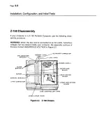
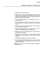
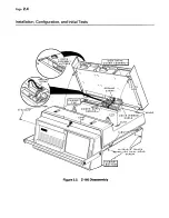
Page 14: ...Page 2 4 Installation Configuration and Initial Tests Figure 2 3 Z 160 Disassembly...

Page 15: ...4 All jumpers should be installed as shown in the figure These jumper positions are detailed below D The two RAM size jumpers J6 and J7 should be in the 2K position D The video control jumpers J2 J3...

Page 16: ...n this jumper is in the pas position 5 VDC is used to light a pixel and ground drives dark pixels When this jumper is in the NEG position ground is supplied to the monitor for all lighted pixels and 5...

Page 17: ...switch setting The following instructions describe resetting these switches Locate the CPU card Figure 2 2 or Figure 2 5 Unplug the keyboard from the back of the computer Unplug the 4 pin connector f...

Page 18: ...firmly push the card into the backplane connector until the card is fully inserted Secure the card to the back of the computer with the screw removed from the blank bracket CAUTION The computer can be...

Page 19: ...d the blank bracket Install the card as follows Align the front edge of the card in the card guide Insert the card into the card guide Line up the card edge connector with the backplane connector Gent...

Page 20: ...on cable and the power supply cable s through the cutout in the cabinet top Slide the front of the cabinet top under the lip in the front panel and then lower the top cover onto the computer Reinstall...

Page 21: ...of both cables are on the same side when connected Connect the power supply cable s Connect the ground strap to the computer frame as shown in the inset Gently lower the disk drive assembly onto the...

Page 22: ...Card o Connect the computer and monitor to electrical power and switch both units on Video can be selected from the Z 329 Card in one of three ways If the CPU is configured for the monochrome display...

Page 23: ...Page 2 13 Installation Configuration and Initial Tests ICOVER I 6 32x3 S Figure 2 10 Z 150 Reassembly...

Page 24: ...itch off the unit and disconnect the power cord and all peripherals from electrical power Remove the screws from the back panel of the computer there are four screws on the PC 2 and PC XT models one i...

Page 25: ...s are detailed below o The two RAM size jumpers J6 and J7 should be in the 2K position o The video control jumpers J2 J3 and J4 all should be in the positive POS position o Vertical sync jumper J1 sho...

Page 26: ...this jumper is in the NEG position ground is supplied to the monitor for all lighted pixels and 5 VDC is used for dark pixels Jumper J2 controls the polarity of the intensity signal In the POS positi...

Page 27: ...SSETTE I O KEYBOARD I O SYSTEM CONFIGURATION DIP SWITCHES CLOCK CHIP TRIMMER SYSTEM BOARD I POWER P1 ECTION P2 o 000000 READ ONLY MEMORY A 000000 o 00000000 0000000 o 00000000 0000000 o 00000000 00000...

Page 28: ...save the blank bracket screw Figure 2 15 from the blank bracket and then remove and discard the blank bracket Install the card as follows Align the front edge of the card in the card guide Insert the...

Page 29: ...lower back corners Proceed to the checkout procedure Checkout D Connect a monitor to the output from the Z 329 Card D Connect the computer and monitor to electrical power and switch both units on D Lo...

Page 30: ......

Page 31: ...SCII data into pixel lighting instructions Memory Organization RAM The memory supplied on the Z 329 consists of two 2K x 8 static RAMs One RAM IC is used to store the character in ASCII code and the o...

Page 32: ...LOCATION CHARACTER ADDRESS ATTRIBUTE ADDRESS 1 BOOOO BOO01 2 BOO02 BOO03 3 BOO04 BOO05 4 BOO06 BOO07 80 last in line 1 BOOAO BOOA1 81 1 st in line 2 BOOA2 BOOA3 1975 1 st in line 25 BOF5E BOF5F 2000...

Page 33: ...cate the bytes re quired to generate the number The character ROM generates the pixel lighting data based on the charac ter stored in RAM and the address from the CRTC Different fonts are possible by...

Page 34: ...manager of the display and as such has priority over the CPU in accessing the RAM The CRTC cannot write to the RAM but controls the transfer from the RAM to the monitor The CPU is allowed to write to...

Page 35: ...rolled by its 18 internal registers All CRTC internal registers are set by the CPU at power up The internal registers are Address Register AR This 5 bit register is used to address the 18 internal reg...

Page 36: ...sed the display shifts to the right The default value is 52H or 82 decimal Sync Width Register R3 This 8 bit write only register sets the pulse width of the sync pulse The horizontal sync is controlle...

Page 37: ...ng when the value for R4 was determined This value is ex pressed in scan lines The correct value is 6 06H Vertical Displayed Register R6 This 7 bit write only register de termines the number of charac...

Page 38: ...f 6 e e 7 EVEN ODD FIELD FIELD INTERLACE MODE o o o o o o o 0 4 000 2 0 3 0 5 0 6 0 7 0 SCAN LINE ADDRESS 0 1 0 Figure 3 2 Interlace Non Interlace Modes Interlace Mode and Skew Register R8 This write...

Page 39: ...3 4 Cursor Skew Delay Control BIT7 o o 1 1 BIT6 o 1 o 1 SKEW No character skew 1 character skew 2 character skew Not available Maximum Scan Line Address Register R9rThis 5 bit write only register cont...

Page 40: ...py the full character field set the lower 5 bits of R10 to scan line 0 and R11 register to scan line 14 14th line Similarly if a single line of the character space is to be used both R10 and R11 would...

Page 41: ...each bit is shown in Table 4 1 Table 4 1 Video Control Register Functions BIT NUMBER DBO DB1 DB2 DB3 SIGNAL NAME BRDEN VIDEN BIT VALUE o x x o FUNCTION Prevents communication between the CPU and the...

Page 42: ...ng of the character These bits control the font in use FONT 1 by the display The font selection follows a standard binary count 00 font 0 01 font 1 10 font 2 11 font 3 Fonts 2 and 3 can be used only i...

Page 43: ...le 4 2 Character Attribute Addressing DISPLAY LOCATION CHARACTER ADDRESS ATIRIBUTE ADDRESS 1 BOOOO BOO01 2 BOO02 BOO03 3 BOO04 BOO05 4 BOO06 BOO07 80 last in line 1 BOOAO BOOA1 81 1 st in line 2 BOOA2...

Page 44: ...Table 4 3 along with the code that generates them In order to blink the character the blink enable bit in the control register must be set as described earlier in this chapter Table 4 3 Attribute Code...

Page 45: ...addresses the two RAMs at the same time there is no correspond ing bit o Character address bit 0 from the CRTC is the same as address bit 1 from the CPU The relationship of the addresses is such that...

Page 46: ...ister To blank the display write XXXX OXX1 for example 01 H to I O address 3B8H No characters will be displayed on the CRT but the RAM may be changed at this time The display is cleared by writing Os...

Page 47: ...eyond the first page so that no addresses beyond the capability of the RAM are used at the end of the page Paging the Display The standard RAM contains only enough memory to display one page of text T...

Page 48: ...r 3 3 3 C S c s 4 4 IT 4 D T d t 5 5 4t CJ o 5 E U e u 6 6 6 F V f v 7 7 1 7 G W g W 8 8 T 8 H X h x 9 9 0 1 9 I Y y 1 10 A 5l Z J X 11 B d K k 12 C Q L L 1 I I 13 D j M ill 14 E N 1 n 15 F C 0 0 D D...

Page 49: ...addresses which can be written to or read from and their use Table 4 6 shows the CRTC registers and their default values Table 4 5 Register Addresses 1 0 ADDRESS 384 385 388 38A FUNCTION CRTC Index R...

Page 50: ...HSYNC Position Characters 52H R3 HSYNCWidth Characters FH R4 Vertical Total Char Rows 19H R5 VTOTAL Adjust Scan Line 6H R6 Vertical Displayed Char Row 19H R7 VSYNC Position Char Row 19H R8 Interlace M...

Page 51: ...rs alphanumeric characters to the Z 329 Card in ASCII code The character and an attribute byte are stored in the RAM on the Z 329 Card When the character is to be displayed the CRTC addresses the memo...

Page 52: ...o the video output CRTC The CRTC provides the sync pulses for the monitor and address information to the RAMs during video cycles The internal registers of the CRTC can be addressed to provide a numbe...

Page 53: ...45 to the RAM When the NIDEO signal is high the CPU addresses are connected to the RAM CRTC 6845 access time is 308 nanoseconds and CPU access time is 245 nanoseconds When the CPU requests a memory ac...

Page 54: ...nal from U31 enables the output allowing data to be sent to the CPU The 6845 CRTC U1 has the most complex read write procedure of all the devices on the monochrome video card because it requires one w...

Page 55: ...ses by octal transceiv ers U2D and U24 The enabling and direction of these transceivers are also controlled by signals from U26 The states of the transceivers are shown in Table 5 1 When a write funct...

Page 56: ...m U29 Note that the data from U15 is read on the fly and may violate data stability bus timing requirements when read Converting Character Data To Pixel Drive Signals The CRTC addresses the RAMs for c...

Page 57: ...he character is formed The output from the character ROM is latched into U8 U8 is a universal shift storage register which is used as a parallel in serial out shift register U8 is described more fully...

Page 58: ...g sent to the monitor on pin 6 of the output connector The BLINK bit from the attribute RAM is delayed by flip flop U27 and then connected to U13 which gates the intensity bit into U15 Sync The horizo...

Page 59: ...which is dedicated to the display The CRTC then controls the transfer of that data from the video memory to the display and provides the sync signals to the CRT The pinout of the 6845 is shown in Fig...

Page 60: ...ory This signal can be used to ena ble memory and or to provide input to memory ac cess arbitration logic This output is used to light the cursor pixels at the correct address 5 VDC must be supplied a...

Page 61: ...the scan line address make up the complete address This output is the horizontal sync to the monitor This signal is derived from the clock signal The frequency and pulse width of this signal can be p...

Page 62: ...e QH output Clearing the 74ALS299 is accomplished by bringing the S1 line low and then bringing the clear line low The hold mode not possible because SO is held high is accomplished by bringing both S...

Page 63: ...c...

Page 64: ...595 3354...

Reviews: