background image

Manual PCIe-DIO-24HS PCI Express Digital I/O Card 

13 

Base Address   +2 (read/write) Port C DIO 
 

Bit 7  Bit 6  Bit 5  Bit 4  Bit 3  Bit 2  Bit 1  Bit 0 
PC7  PC6  PC5  PC4  PC3  PC2  PC1  PC0 

Table 5-4: 

Base +2 Port C DIO


Reading from this address will return the digital data on Port C.  Writing to this address will 
output the digital data on Port C.  Readback is supported while in output mode.  Port C can 
also be broken into two nybbles, Port C Low (bits 0-3), and Port C High (bits 4-7). Each nybble 
can be independently set as input or output.  Base A3 controls Port C's I/O direction. 

 
Base Address   +3 (read/write) Control Register 


The DIO function contains a control register. This 8-bit register is used to set the direction of 
the Ports. At power-up or reset, all DIO lines are automatically set as inputs and should be 
configured during initialization by writing to the control register even if the Ports are going to 
be used as inputs.  Bit 7 must be set to 

‘1’ when configuring the direction of the Ports.  This 

register can be readback with bits 2, 5, 6, and 7 always reading zero.   


Ports can be written to while configured as inputs.  When a Port is changed from input 
to output, the last written value will be applied.  If a Port has never been written to, the 
value on the Port's pins while in input mode will be applied to the Port when configured 
as an output.  This prevents the Ports pins from glitching when set as outputs. 


Bit


Assignment


Code


D0 

Port C Lo (C0-C3)  1=Input, 0=Output 

D1 

Port B 

1=Input, 0=Output 

D2 

Reserved 

Set to 

‘0’ 

D3 

Port C Hi (C4-C7) 

1=Input, 0=Output 

D4 

Port A 

1=Input, 0=Output 

D5,D6 

Reserved 

Set to “00” 

D7 

Direction Set Flag  1=Active 

Table 5-5: 

Base +3, DIO Port Direction Control Register 


Base Address   +4 t9 Not Used 


Base Address   +A (read/write) DIO Buffer Enable / Disable (tri-state) 

 
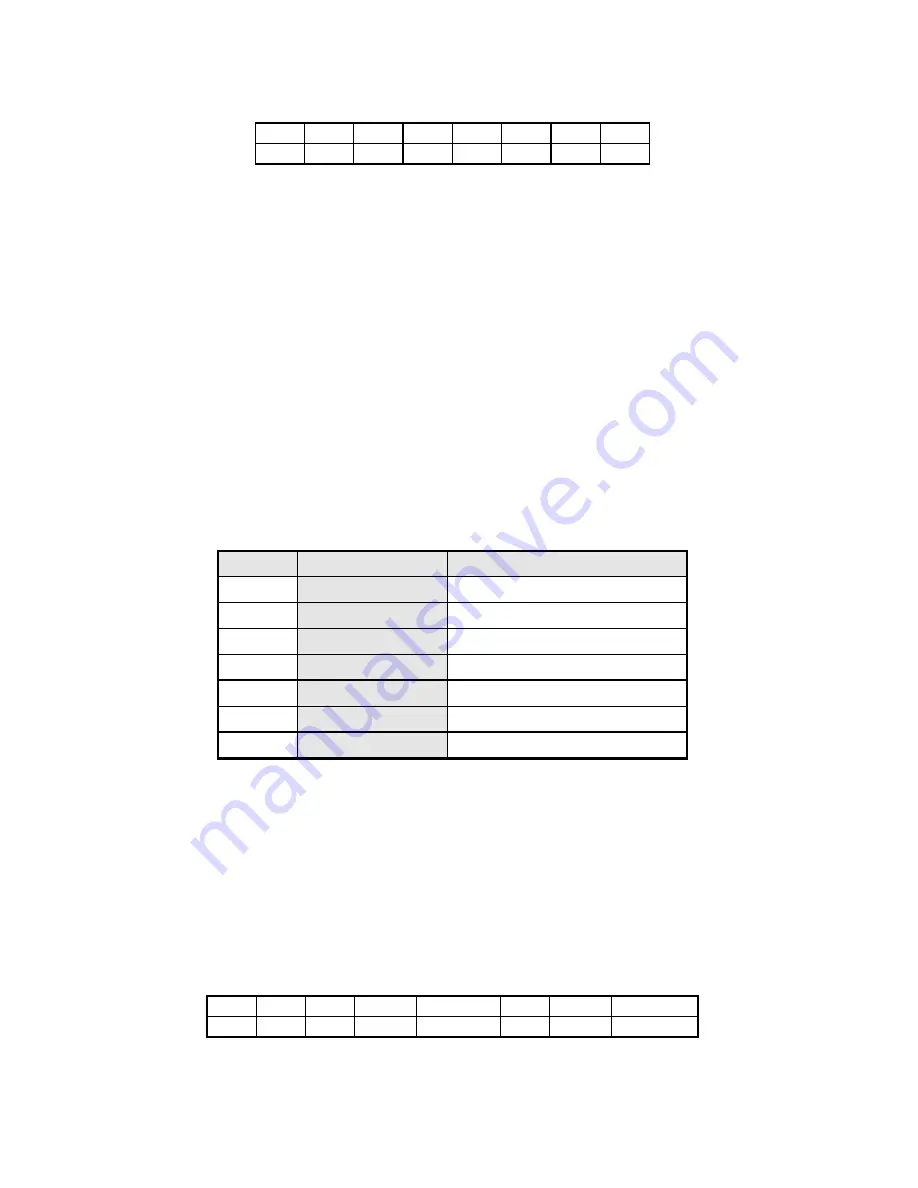
At power-up or reset, all DIO buffers on the card are enabled. To globally disable the DIO 
buffers write a one to bit 0.  To globally re-enable the DIO buffers, write a zero to bit 1.  When 
the buffers are disabled the connector pins are tri-stated and biased by the state of the pull up 
or down configuration jumper.  A read returns the buffer status; 0=enabled, 1=disabled. 
 

Bit 7  Bit 6  Bit 5 

Bit 4 

Bit 3 

Bit 2 

Bit 1 

Bit 0 

‘0’ 

‘0’ 

‘0’ 

Port A  Port C Hi 

‘0’ 

Port B  Port C Lo 

Table 5-6

: Base +A, DIO Buffer Enable 


Summary of Contents for PCIe-DIO-24HS

Page 1: ...Diego CA 92121 858 550 9559 Fax 858 550 7322 contactus accesio com www accesio com MODELS PCIe DIO 24HS PCIe DIO 24H PCI Express 24 Channel Digital I OCard with Change of State Detection USER MANUAL...

Page 2: ...t rights of ACCES nor the rights of others IBM PC PC XT and PC AT are registered trademarks of the International Business Machines Corporation Printed in USA Copyright 2015 by ACCES I O Products Inc 1...

Page 3: ...ge for labor or parts not excluded by warranty Warranty commences with equipment shipment Following Years Throughout your equipment s lifetime ACCES stands ready to provide on site or in plant service...

Page 4: ...nnector Pin Assignments 15 Chapter 7 Specifications 17 Customer Comments 18 LIST OF FIGURES Figure 1 1 Block Diagram 6 Figure 3 1 Option Selection Map 9 Figure 6 1 50 Pin Male Header 15 LIST OF TABLES...

Page 5: ...bit Ports independently selectable for inputs or outputs Pull up resistors on DIO lines user configurable pull down 5V VCCIO 3 3V user configurable Fused VCCIO voltage available to the user on I O he...

Page 6: ...sabling and clearing the interrupts Each DIO line is buffered and capable of sourcing 32mA or sinking 64mA The VCCIO level is 5V or can be configured as 3 3V By default the DIO lines are pulled up wit...

Page 7: ...ick disconnect grounding tab on the mounting bracket Factory Options Extended temperature operation 40 to 85 C RoHS compliant version Optional Accessories CAB50F 6 Six foot ribbon cable assembly with...

Page 8: ...TART RUN and type click OK or press c Follow the on screen prompts to install the software for this board Linux a Please refer to linux htm on the CD for information on installing under Linux Hardware...

Page 9: ...anual VCC Select Position the jumper to select either 5VTTL logic or 3 3VDC logic Figure 3 1 Option Selection Map Bias Select Select 10k ohm pull up or pull down resistors per port using the provided...

Page 10: ...cts to pin 49 of the I O connector and is used to protect the card and PC power supply when used to power external module racks relay boards or for general purposes If an over current persists on a ci...

Page 11: ...each function on each of the cards and the respective IRQs Alternatively Windows systems can be queried to determine which resources were assigned In these operating systems you can use either PCIFin...

Page 12: ...e Address E Port C bit 3 IRQ Enable Read Write Base Address F IRQ Clear Write Table 5 1 Register Address Map Base Address 0 read write Port A DIO Bit 7 Bit 6 Bit 5 Bit 4 Bit 3 Bit 2 Bit 1 Bit 0 PA7 PA...

Page 13: ...7 always reading zero Ports can be written to while configured as inputs When a Port is changed from input to output the last written value will be applied If a Port has never been written to the val...

Page 14: ...lobal Write any value to this address to disable all IRQ sources on the card Base Address E read write IRQ Enable Port C bit 3 Bit 7 Bit 6 Bit 5 Bit 4 Bit 3 Bit 2 Bit 1 Bit 0 0 0 IRQ Output 1 0 0 0 C3...

Page 15: ...e Pin Signal Name 1 PC7 2 GND 3 PC6 4 GND 5 PC5 6 GND 7 PC4 8 GND 9 PC3 10 GND 11 PC2 12 GND 13 PC1 14 GND 15 PC0 16 GND 17 PB7 18 GND 19 PB6 20 GND 21 PB5 22 GND 23 PB4 24 GND 25 PB3 26 GND 27 PB2 28...

Page 16: ...C bit 0 PB7 I O Port B bit 7 PB6 I O Port B bit 6 PB5 I O Port B bit 5 PB4 I O Port B bit 4 PB3 I O Port B bit 3 PB2 I O Port B bit 2 PB1 I O Port B bit 1 PB0 I O Port B bit 0 PA7 I O Port A bit 7 PA6...

Page 17: ...2uA 0 8V 2uA High Inputs 3 5V 2uA 2 0V 2uA Low Outputs 0 55V 32mA 0 55V 24mA High Outputs 3 8V 32mA 2 4V 24mA Table 7 1 VCCIO Logic Levels Power Output VCCIO P3 pin 49 Environmental Operating Temperat...

Page 18: ...ems with this manual or just want to give us some feedback please email us at manuals accesio com Please detail any errors you find and include your mailing address so that we can send you any manual...

Reviews: