Programmer’s Model
2-32
Copyright © ARM Limited 2000. All rights reserved.
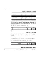
With the cache debug index register (CP15 r15), you can access any location within the
instruction or data cache. You must program this register before using any of the TAG
or cache read/write operations. The cache debug index register provides an index into
the cache memories.
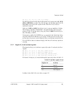
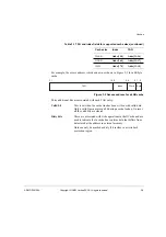
The format of the index/segment data is shown in Figure 2-5.
Figure 2-5 Index/segment format
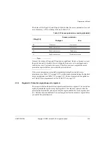
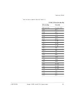
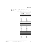
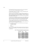
The size of the index varies depending on the implemented cache size. Table 2-20
shows how the index address field size changes for the cache sizes supported by the
ARM946E-S.
Note
For TAG operations, the word address field in the cache debug register is ignored.
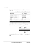
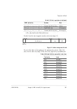
The data format for the TAG read/write operations is shown in Figure 2-6.
Figure 2-6 Data format TAG read/write operations
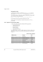
Data TAG read
Data
MRC p15, 3, rd, c15, c2, 0
Instruction cache write
Data
MCR p15, 3, rd, c15, c3, 0
Instruction cache read
Data
MRC p15, 3, rd, c15, c3, 0
Data cache write
Data
MCR p15, 3, rd, c15, c4, 0
Data cache read
Data
MRC p15, 3, rd, c15, c4, 0
Table 2-27 Additional operations (continued)
Function
Data
Instruction
31 30 29
N+1 N
5 4
2 1 0
Should be zero
Index
Word
address SBZ
Segment
31
N+1 N
5 4 3 2 1 0
TAG address
Index
Dirty
bits Set
Valid
Summary of Contents for ARM946E-S
Page 1: ...ARM DDI 0155A ARM946E S Technical Reference Manual ...
Page 6: ...vi Copyright ARM Limited 2000 All rights reserved ARM DDI 0155A 04 Limited Confidential ...
Page 54: ...Programmer s Model 2 34 Copyright ARM Limited 2000 All rights reserved ARM DDI 0155A ...
Page 70: ...Caches 3 16 Copyright ARM Limited 2000 All rights reserved ARM DDI 0155A ...
Page 78: ...Protection Unit 4 8 Copyright ARM Limited 2000 All rights reserved ARM DDI 0155A ...
Page 112: ...Coprocessor Interface 7 14 Copyright ARM Limited 2000 All rights reserved ARM DDI 0155A ...


