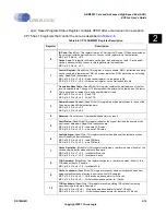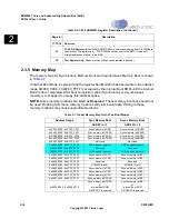
DS785UM1
2-17
Copyright 2007 Cirrus Logic
ARM920T Core and Advanced High-Speed Bus (AHB)
EP93xx User’s Guide
2
2
2
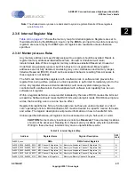
Note: The shaded memory areas are dedicated to system registers. Details of these registers
are in
.
2.3.6 Internal Register Map
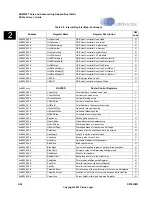
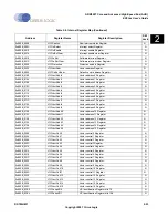
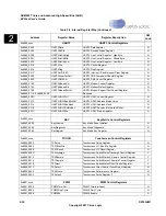
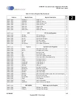
shows the memory map for internal registers. Registers are set to
their default state by the
RSTOn
pin input or by the
PRSTn
pin input. Some state conserving
registers are reset only by the
PRSTn
pin.
All registers are read/write unless otherwise
specified.
2.3.6.1 Memory Access Rules
Any memory address not specifically assigned to a register should be avoided. Reads to
register memory addresses labelled Reserved, Unused or Undefined will return
indeterminate data. Writes to register memory addresses labelled Reserved, Unused or
Undefined are generally ignored, but this behavior is not guaranteed. Many register
addresses are not fully decoded, so aliasing may occur. Addresses and memory ranges
listed as Reserved (RSVD) should not be accessed; behavior resulting from accesses to
these regions is not defined.
The SW Lock field identifies registers with a software lock. A software lock prevents the
register from being written (unless an unlock operation is performed immediately prior to the
write). Any register whose accidental alteration could cause system damage may be
controlled with a software lock. Each peripheral with software lock capability has its own
software lock register.
Within a register definition, a reserved bit indicated by the name RSVD, means the bit is not
accessible. Software should mask the RSVD bits when doing bit reads. RSVD bits will ignore
writes, that is writing a zero or a one has no affect.
Register bits identified as NC are functionally alive but have an undocumented or a “don’t
care” operating function. Bits identified as NC must be treated in a specific manner for reads
and writes. The register descriptions will provide information on how to handle NC bits.
Unless specified otherwise, all registers can be accessed as a byte, half-word, or word.
CAUTION: Some memory locations are listed as Reserved. These memory locations
should not be accessed. Reading from these memory locations will yield invalid data.
Writing to these memory locations may cause unpredictable results.
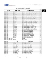
Table 2-8. Internal Register Map
Address
Register Name
Register Description
SW
Lock
0x8000_xxxx
DMA
DMA Control Registers
0x8000_0000 - 0x8000_003C
M2P Channel 0 Registers (Tx)
Memory-to-Peripheral Channel 0 Registers (Tx)
N
0x8000_0040 - 0x8000_007C
M2P Channel 1 Registers (Rx)
Memory-to-Peripheral Channel 1 Registers (Rx)
N
0x8000_0080 - 0x8000_00BC
M2P Channel 2 Registers (Tx)
Memory-to-Peripheral Channel 2 Registers (Tx)
N
0x8000_00C0 - 0x8000_00FC
M2P Channel 3 Registers (Rx)
Memory-to-Peripheral Channel 3 Registers (Rx)
N
0x8000_0100 - 0x8000_013C
M2M Channel 0 Registers
Memory-to-Memory Channel 0 Registers
N
Summary of Contents for EP93 Series
Page 28: ...P 6 DS785UM1 Copyright 2007 Cirrus Logic Preface EP93xx User s Guide PP P ...
Page 162: ...5 36 DS785UM1 Copyright 2007 Cirrus Logic System Controller EP93xx User s Guide 55 5 ...
Page 576: ...15 18 DS785UM1 Copyright 2007 Cirrus Logic UART2 EP93xx User s Guide 1515 15 ...
Page 634: ...17 38 DS785UM1 Copyright 2007 Cirrus Logic IrDA EP93xx User s Guide 1717 17 ...
Page 648: ...19 6 DS785UM1 Copyright 2007 Cirrus Logic Watchdog Timer EP93xx User s Guide 1919 19 ...
Page 688: ...21 32 DS785UM1 Copyright 2007 Cirrus Logic I2S Controller EP93xx User s Guide 2121 21 ...
Page 790: ...27 20 DS785UM1 Copyright 2007 Cirrus Logic IDE Interface EP93xx User s Guide 2727 27 ...
Page 808: ...28 18 DS785UM1 Copyright 2007 Cirrus Logic GPIO Interface EP93xx User s Guide 2828 28 ...


