background image

GR-CPCI-GR740-QSG
June 2017, Version 1.4

24

www.cobham.com/gaisler

For the other IOs you will have to make a system-level decision as to whether you can tolerate some IO interfaces
toggling during boot-up, and if not, you could use one of the GPIOs to drive an enable signal to those IO interfaces
transceivers to disable them during boot. Please note that this is not supported currently on the GR-CPCI-GR740
development board.

6.11. Can't boot

First,  check  that  the  BREAK  button  is  not  asserted  (should  be  in  the  rightmost  position).  Second,  check  that
your boot image is properly loaded into the flash memory (starting address 0xc0000000). You can use the verify
command of GRMON2 that will do it for you. Third, make sure that both memory controllers (mctrl0 and sdctrl0)
are properly initialized. To check if that is happening, you can connect with GRMON2 with no initialization flag (-
ni) once your system has been powered up. For instance, using JTAG/FTDI debug link, the command is "grmon -
ftdi -ni". Please note, that if you use GRMON2 without the "ni" flag, GRMON2 initializes both memory controllers
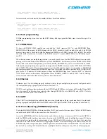
and thus, the state left by your boot code cannot be analysed. Once in grmon, check the value of the memory
controller configuration registers, as shown below:

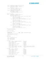
grmon2> info reg -v mctrl0

  Memory controller with EDAC

      0xff903000  Memory config register 1                0x0803c0ff

      30     pbrdy             0x0         PROM area bus ready enable             

      29     abrdy             0x0         Asynchronous bus ready enable          

      28:27  iobusw            0x1         I/O bus width                          

      26     ibrdy             0x0         I/O bus ready enable                   

      25     bexcn             0x0         Bus error enable                       

      23:20  iows              0x0         I/O wait states                        

      19     ioen              0x0         I/O enable                             

      17:14  prombanksz        0xf         PROM bank size                         

      11     pwen              0x0         PROM write enable                      

       9:8   promwidth         0x0         PROM width                             

       7:4   promwws           0xf         PROM write wait states                 

       3:0   promrws           0xf         PROM read wait states                  


      0xff903004  Memory config register 2                0x00000020

      31     sdramrf           0x0         SDRAM refresh enable                   

      30     sdramtrp          0x0         SDRAM TRP parameter                    

      29:27  sdramtrfc         0x0         SDRAM TRFC parameter                   

      26     sdramtcas         0x0         SDRAM TCAS parameter                   

      25:23  sdrambanksz       0x0         SDRAM bank size                        

      22:21  sdramcolsz        0x0         SDRAM column size                      

      20:19  sdramcmd          0x0         SDRAM command                          

      18     d64               0x0         SDRAM 64-bit data bus                  

      17     sdpb              0x0         SDRAM page burst                       

      14     se                0x0         SDRAM enable                           

      13     si                0x0         SRAM disable                           

      12:9   rambanksz         0x0         RAM bank size                          

       7     rbrdy             0x0         RAM bus read enable                    

       6     rmw               0x0         Read-modify-write enable               

       5:4   ramwidth          0x2         RAM width                              

       3:2   ramwws            0x0         RAM write wait states                  

       1:0   ramrws            0x0         RAM read wait states                   


      0xff903008  Memory config register 3                0x08000000

      28     rse               0x0         Reed-Solomon EDAC enable               

      27     me                0x1         Memory EDAC available                  

      26:12  sdramreload       0x0         SDRAM refresh counter reload value     

      11     wb                0x0         EDAC diagnostic write bypass enable    

      10     rb                0x0         EDAC diagnostic read bypass enable     

       9     re                0x0         RAM EDAC enable                        

       8     pe                0x0         PROM EDAC enable                       

       7:0   tcb               0x0         Test checkbits                         


      0xff903010  Memory config register 5                0x00000000

      29:23  iohws             0x0         IO lead out                            

      13:7   romhws            0x0         ROM lead out                           


      0xff903014  Memory config register 6                0x00000000

      13:7   ramhws            0x0         RAM lead out                           


      0xff903018  Memory config register 7                0x00000000

      31:16  brdyncnt          0x0         Bus ready count                        

      15:0   brdynrld          0x0         Bus ready reload value                 


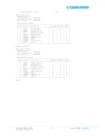
grmon2> info reg -v sdctrl0

  PC133 SDRAM Controller

      0xffe00000  SDRAM config register                   0xfea087a4

      31     refresh           0x1         SDRAM refresh enable                   

Summary of Contents for GR-CPCI-GR740

Page 1: ...740 A development board based on the GR740 processor 2017 User s Manual The most important thing we build is trust GR CPCI GR740 Quick Start Guide GR CPCI GR740 QSG 1 www cobham com gaisler June 2017...

Page 2: ...Running binaries linked to address 0x40000000 11 3 5 Considerations when enabling the Level 2 cache 11 4 GRMON2 hardware debugger 12 4 1 Overview 12 4 2 Debug link alternatives 12 4 2 1 Connecting vi...

Page 3: ...possibly newer revisions are available from the GR CPCI GR740 product page at http www gaisler com 1 2 References Table 1 1 References RD 1 GR CPCI GR740 Development Board User s Manual RD 2 GR740 Da...

Page 4: ...source is required for the PCI interface which can operate at 33 or 66 MHz either from the PCI backplane or from an oscillator in socket X3 PCICLK Please refer to GR CPCI GR740 Development Board User...

Page 5: ...ignal FP S3 1 controls if the design s Debug Support Unit is enabled and also if the debug communication links are active DIP switch S3 1 must be set to OPEN i e DSU enabled to connect to the board us...

Page 6: ...DAC and enable PROM mode FP S3 1 Open to enable DSU FP S3 2 Open to have external memory clock FP S3 3 FP S3 4 FP S3 5 Closed to enable PLLs and FP S3 6 Open to ignore PLL lock FP S3 7 to Closed to en...

Page 7: ...8 15 This means that the PROM IO can only be used in 8 bit mode up to 16 MiB instead of 64 MiB when using the UART0 and UART1 along with the PROM because the MSB address pins and the MSB data pins of...

Page 8: ...ce shares pins with PCI and Ethernet port 1 There are three configurations a 96 bit memory interface b 48 bit memory interface and PCI and c 48 bit memory interface and Ethernet port 1 These configura...

Page 9: ...PCI GR740 Development Board User s Manual Default configuration The default configuration uses only ethernet port 0 prepared to use EDCL by setting FP S2 1 and FP S2 2 Open see Figure 2 2 But disabled...

Page 10: ...ion MIL STD 1553 Interface of the GR CPCI GR740 Development Board User s Manual 2 6 7 Spacewire There are nine Spacewire SPW interfaces provided by the GR740 that can be connected on the front panel w...

Page 11: ...ng over AHB to AHB bridges the qambapp must be specified The functionality enabled by qambapp is enabled by default starting with BCC version 1 0 41 With version 1 0 41 or higher of BCC the following...

Page 12: ...necting via the FTDI USB JTAG interface Please see Section 2 6 1 to configure FTDI interface Please see GRMON User s Manual for how to set up the required FTDI driver software Then connect the PC and...

Page 13: ...mand more details about the system is printed and with info reg the register contents of the I O registers can be inspected Below is a list of items of particular interest AMBA system frequency is pri...

Page 14: ...AHB Status Register Cobham Gaisler General Purpose I O port Cobham Gaisler General Purpose Register Cobham Gaisler Temperature sensor Cobham Gaisler General Purpose Register Bank Cobham Gaisler CCSDS...

Page 15: ...line lru snoop tags CPU3 win 8 hwbp 2 itrace 512 V8 mul div srmmu lddel 1 GRFPU FT stack pointer 0x0ffffff0 icache 4 4 kB 32 B line lru dcache 4 4 kB 32 B line lru snoop tags apbmst0 Cobham Gaisler AH...

Page 16: ...PW Router DMA interface APB FF90F000 FF910000 IRQ 22 Number of ports 1 grspw4 Cobham Gaisler GRSPW Router DMA interface APB FF910000 FF911000 IRQ 23 Number of ports 1 greth0 Cobham Gaisler GR Ethernet...

Page 17: ...rmmu lddel 1 GRFPU FT stack pointer 0x0ffffff0 icache 4 4 kB 32 B line lru dcache 4 4 kB 32 B line lru snoop tags grmon2 l2cache invalidate invalidate all cache lines grmon2 l2cache enable grmon2 load...

Page 18: ...1 6 L4STAT LEON4 Statistics 0 0 1 7 APBUART UART 0 0 1 0 8 APBUART UART 1 0 1 0 9 SPICTRL SPI Controller 0 0 1 10 MCTRL PROM IO 0 1 0 grmon2 grcg enable 4 grmon2 grcg clkinfo GRCLKGATE GR740 info Unlo...

Page 19: ...e the memory modules you must check if this setup still applies 2 Enable 2T signaling on memory controller SDCTRL This improves the SDRAM signal timing required for some memory modules 3 Initialize me...

Page 20: ...ded stream length 13454 bytes Compression Ratio 1 825 section data at 0x5ff0 size 2912 bytes Uncoded stream length 2912 bytes Coded stream length 827 bytes Compression Ratio 3 521 creating LEON3 boot...

Page 21: ...simplest way to obtain new parameters is to connect to the design with GRMON2 and issue info reg and copy the values that GRMON2 has initialized the SDRAM memory controller with The stack and ramsize...

Page 22: ...n values in the cache s internal memories may be interpreted as valid cache data The Level 2 cache contents can be invalidated and the cache then enabled with the following GRMON2 sequence grmon2 l2ca...

Page 23: ...use the PROM_ADDR 20 22 pins for the 1553 interface For that purpose change the MKPROM flags from romsize 8192 to romsize 1024 Please note that this custom configuration leaves PROMIO_ADDR 21 and 20...

Page 24: ...bus ready enable 25 bexcn 0x0 Bus error enable 23 20 iows 0x0 I O wait states 19 ioen 0x0 I O enable 17 14 prombanksz 0xf PROM bank size 11 pwen 0x0 PROM write enable 9 8 promwidth 0x0 PROM width 7 4...

Page 25: ...6 Check that the GPIO ribbon cable that goes from the front panel to the PCB J4 connector is properly connected see Figure 6 1 Sometimes this connector moves a little bit out due to movement of the b...

Page 26: ...n full including company affiliation and site name and address Please identify exactly what product that is used specifying if it is an IP core with full name of the library distribution archive file...

Page 27: ...ed JP5 1 2 3 4 connected 5 6 disconnected JP6 All connected except 1 2 JP7 All disconnected JP8 Connected JP9 Connected JP10 Disconnected JP11 1 2 13 and 14 in position B C The rest in position A B JP...

Page 28: ...h Default configuration FP S2 2 Pull up FP S2 3 Pull down FP S2 4 Pull up FP S2 5 Pull up FP S2 6 Pull up FP S2 7 Pull down FP S2 8 Pull down FP S3 1 Open FP S3 2 Open FP S3 3 Closed FP S3 4 Closed FP...

Page 29: ...is document is current before using this product Cobham does not assume any responsibility or liability arising out of the application or use of any product or service described herein except as expre...

Reviews: