3.5.3 MCU Serial Peripheral Interface (3-wire SPI)
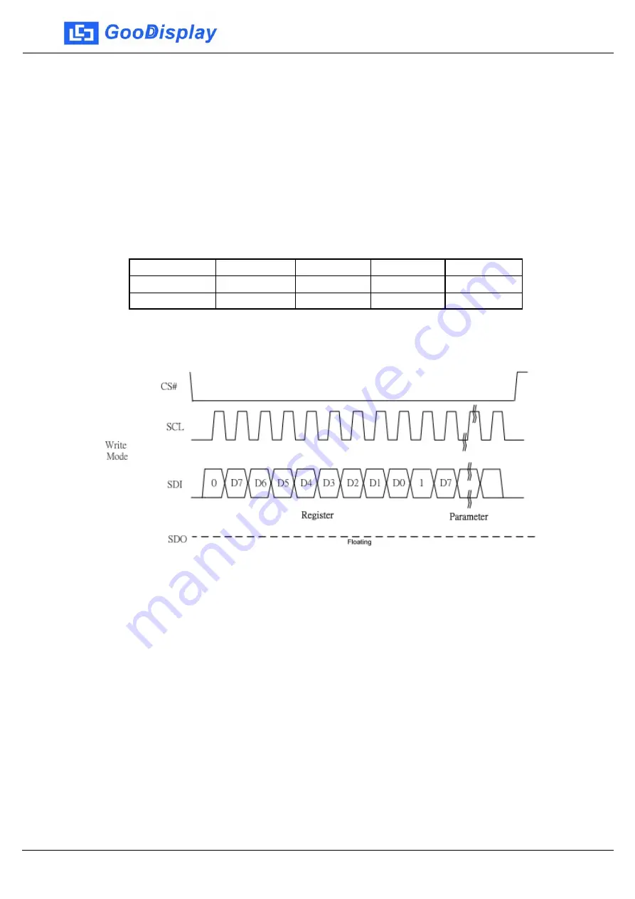
The 3-wire SPI consists of serial clock SCL, serial data input SDI, and CS#. The
operation is similar to 4- wire SPI while D/C# pin is not used and it must be tied to
LOW. The control pins status in 3-wire SPI is shown in Table 3.5-3.
In the write operation, a 9-bit data will be shifted into the shift register on every
clock rising edge. The bit shifting sequence is D/C# bit, D7 bit, D6 bit to D0 bit.
The first bit is D/C# bit which determines the following byte is command or data.
When D/C# bit is 0, the following byte is command. When D/C# bit is 1, the
following byte is data. Table 3.5-3 shows the write procedure in 3-wire SPI
Table 3.5-3 : Control pins status of 3-wire SPI
Function
SCL pin
SDI pin
D/C# pin
CS# pin
Write command
↑
Command bit
Tie LOW
L
Write data
↑
Data bit
Tie LOW
L
Note:
(1) L is connected to VSS and H is connected to VDDIO
(2)
↑
stands for rising edge of signal
Figure 3.5-3: Write procedure in 3-wire SPI mode
GDEH075Z90
18
/
38
7.5 inch Series
www.good-display.com
GOOD DISPLAY


