92
CHAPTER 3 INTERRUPT
3.10 Sample Program of Interrupt Processing
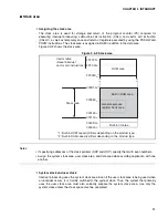
A sample program for interrupt processing is shown below.
■
Sample program for interrupt processing
❍
Processing specification
An example of an interrupt program using external interrupt 0 (INT0) is shown.
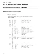
Sample coding from the program is shown below.
[Coding example]
DDR1 EQU 000011H ;Port 1 direction register
ENIR EQU 028H ;Interrupt/DTP enable register
EIRR EQU 029H ;Interrupt/DTP flag
ELVR EQU 02AH ;Request level set register
ICR00 EQU 0B0H ;Interrupt control register
STACK SSEG ;Stack
RW 100
STACK_T RW 1
STACK ENDS
;-----------Main program----------------------------------------------------------
CODE CSEG
START:
MOV RP,#0 ;General-purpose register use of
header bank
MOV ILM,#07H ;PS:ILM is set to level 7
MOV A,#!STACK_T ;Setting of system stack
MOV SSB,A
MOVW A,#STACK_T ;Setting of stack pointer, where
MOVW SP,A ;it is set to SSP since S-flag = 1
MOV DDR1,#00000000B ;P10/INT0 pin is set to input
OR CCR,#40H ;I-flag in PS:CCR is set for interrupt enable
MOV I:ICR00,#00H ;Interrupt set to level 0 (highest)
MOV I:ELVR,#00000001B ;INT0 is set to H-level request
MOV I:EIRR,#00H ;INT0 interrupt factor cleared
MOV I:ENIR,#01H ;INT0 input enable
:
LOOP: NOP ;Dummy loop
NOP
NOP
NOP
BRA LOOP ;Unconditional jump
;-----------Interrupt program--------------------------------------------
ED_INT1:
MOV I:EIRR,#00H ;Prohibition of acceptance of new
;INT0
NOP
NOP
NOP
NOP
NOP
NOP
RETI ;Return from interrupt
CODE ENDS
;-----------Vector setting--------------------------------------------------------
VECT CSEG ABS=OFFH
ORG OFFDOH ;Vector is set to interrupt #11(0BH)
DSL ED_INT1
ORG OFFDCH ;Reset vector setting
DSL START
DB 00H ;Set to single chip mode
VECT ENDS
END START
Summary of Contents for MB90480 Series
Page 2: ......
Page 4: ......
Page 10: ...vi ...
Page 128: ...106 CHAPTER 4 RESET ...
Page 174: ...152 CHAPTER 6 LOW POWER CONSUMPTION MODE ...
Page 198: ...176 CHAPTER 7 MODE SETTING ...
Page 220: ...198 CHAPTER 9 TIMEBASE TIMER ...
Page 238: ...216 CHAPTER 11 WATCH TIMER ...
Page 280: ...258 CHAPTER 12 16 BIT INPUT OUTPUT TIMER ...
Page 406: ...384 CHAPTER 17 8 10 BIT A D CONVERTER ...
Page 478: ...456 CHAPTER 20 CHIP SELECTION FACILITY ...
Page 494: ...472 CHAPTER 21 ADDRESS MATCH DETECTION FUNCTION ...
Page 498: ...476 CHAPTER 22 ROM MIRROR FUNCTION SELECTION MODULE ...
Page 526: ...504 CHAPTER 23 2M 3M BIT FLASH MEMORY ...
Page 536: ...514 CHAPTER 24 EXAMPLES OF MB90F481B MB90F482B MB90F488B MB90F489B SERIAL PROGRAMMING ...
Page 570: ...548 CHAPTER 25 PWC TIMER ONLY MB90485 SERIES ...
Page 688: ......

