background image

DIGITAL CLOCK MODEL CLK036


GEKCO INC.  


Rev 1.0  


17


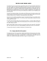
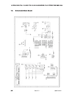
The crystal Y1 provides the clock for the microcontroller and C1 and C2 are required pad capacitors for 
the crystal to operate. The display board interface connectors are J4 and J5. J5 is the only one used in 
the model CLK036. This connector provides the standard serial peripheral interface (SPI) interface to 
the display board. The signal SS is asserted low when serial data is present on the MISO signal. The 
MISO signal is the serial data stream from the microcontroller to the MAX7219 on the display board. 
The  signal  SCK  provides  the  clock  timing  for  the  interface.  More  details  of  the  SPI  interface  can  be 
found on the web. 

Connector J3 provides the interface to the real time clock (RTC) module. The clock time accuracy and 
the time keeping function are provided by the RTC module, which has a Maxim DS3231 real time clock. 
This device uses a 3 wire, I2C interface to communicate with the microcontroller. 

Connector J2 is the programming interface connector. This allows the firmware to be modified and the 
ability to reprogram the microcontroller. The CLK036 main board looks just like a Arduino Uno and can 
use the popular Arduino IDE. 

The path for the input power for the clock is provided by connector J1. The input voltage should be 5V 
+/- 5%. Diode D1 is a schottky diode which provides protection of the internal circuits if the polarity of 
the applied voltage is incorrect. 

Resistor network RN1 provides the 10kohm pull up resistors for the switch inputs SW1 through SW4. 
SW1, SW2 and SW3 provide the clock setup capabilities and SW4 allows the user to reset the device. 

The piezo electric buzzer LS1 provides an audible alert for the alarm function.   


11.2.


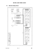
Display Board Circuit Description 

The display board used in the model CLK036 utilizes the MAX7219 as the display driver and controller. 
This  part  provides  a  4  wire  interface  to  the  main  board  to  interface  to  the  8  digit  display.  The  LED 
displays  are  multiplexed  by  the  logic  in  the  MAX7219.  The  microcontroller  on  the  main  board  only 
needs to communicate with the display board when a change in the display is desired. 

Summary of Contents for CLK036

Page 1: ...SW Cypress Ln McMinnville OR 97128 503 472 4770 P N 595 324 REV 1 0 Copyright 2018 GEKCO Inc All Rights Reserved Printed in the United States of America c GEKCO DIGITAL CLOCK MODEL CLK036 ASSEMBLY OP...

Page 2: ...This page is intentionally left blank...

Page 3: ...2 ASSEMBLY 9 4 3 SOLDERING 9 5 STEP BY STEP ASSEMBLY 10 5 1 MAIN CIRCUIT BOARD 10 6 INITIAL TESTS 12 7 FINAL TESTS 13 8 IN CASE OF DIFFICULTY 13 9 FINAL PCA ASSEMBLY 13 10 FINAL ASSEMBLY 13 11 THEORY...

Page 4: ...URE 3 MAIN BOARD TOP VIEW 2 10 FIGURE 4 MAIN BOARD TOP VIEW 3 10 FIGURE 5 MAIN BOARD TOP VIEW 4 11 FIGURE 6 MAIN BOARD WITH STANDOFFS 11 FIGURE 7 MAIN AND DISPLAY BOARD INTERFACE CONNECTOR MOUNTING 12...

Page 5: ...in electronics can be successful but the more experienced builder can skip any unnecessary information Also this design is fully open source for both the hardware and firmware There are full schemati...

Page 6: ...avoid misplacing parts 3 1 Top Level Parts List Remove the parts from the main bag and separate each individual parts bags ITEM QTY PART NO DESCRIPTION 1 1 DBR836 KIT Clock Display Board PCA parts ki...

Page 7: ...20 104 Cap mono Cer 50v radial lead 0 1UF 2 2 C1 C2 21 220 Cap mono Cer COG radial lead 22pF 100v 3 1 C3 26 102 Cap elect alum radial lead 10uF 16v 4 1 Y1 404 160 Crystal HC49 16 00 MHz 5 1 D1 55 62...

Page 8: ...DIGITAL CLOCK P N CLK036 ASSEMBLY OPERATION MANUAL 6 REV 1 0 GEKCO INC 15 1 LS1 220 1420 Audio Piezo Transducer 30V 16 1 81 180912C Printed Circuit Board Main Board 1 2 3 4 5 6 7 8 9 10 11 12 13 14 1...

Page 9: ...LK036HDW KIT ITEM QTY PART NO DESCRIPTION 1 2 255 25511 Hardware Standoff Nylon M3 x 12 mm 2 2 255 29346 Hardware Screw Nylon M3 x 0 50 mm Thread 16mm White 3 2 255 29347 Hardware Screw Nylon M3 x 0 5...

Page 10: ...KIT ITEM QTY PART NO DESCRIPTION 1 1 86 18111901 Front Panel Acrylic 3mm Transparent Red 2 1 86 18111902 Back Panel Acrylic 3mm Clear 3 1 86 18111903 Top Panel Acrylic 3mm Clear 4 1 86 18111904 Botto...

Page 11: ...rations you will perform while assembling your kit A good solder connection will form an electrical connection between two parts such as a component lead and a circuit board foil A bad solder connecti...

Page 12: ...3 Main Board Top View 2 C1 22 pF 22 radial lead ceramic capacitor C2 22 pF 22 radial lead ceramic capacitor In the next step be sure to observe the correct polarity as noted before and lay the capacit...

Page 13: ...e aligned with the silkscreen outline J1 Connector Power 2 1 mm LS1 Audio Piezo Speaker Solder the leads to the foil and cut off the excess lead lengths The next step is to install the mating connecto...

Page 14: ...llowing IC s on the main circuit board CAUTION Integrated circuits IC s are complex electrical devices that perform many complicated operations in a circuit These devices can be damaged during install...

Page 15: ...ority of kits that fail are due to poor solder connections Therefore you can eliminate many difficulties by carefully inspecting each connection to make sure it is soldered as described in the solder...

Page 16: ...of the enclosure onto the main board assembly Make sure the switches properly align with the top piece of the enclosure Figure 10 Enclosure Back with Top Add the main board assembly with the top panel...

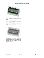
Page 17: ...ing holes Add the front panel and make sure all pieces are aligned properly Add two black screws and loosely tighten to secure the enclosure Congratulations you have successfully completed the assembl...

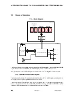
Page 18: ...display boards which could vary in size If may be helpful to review the block diagram and schematics while reading the circuit descriptions 11 1 Main Board Circuit Description The main circuit board h...

Page 19: ...tor J2 is the programming interface connector This allows the firmware to be modified and the ability to reprogram the microcontroller The CLK036 main board looks just like a Arduino Uno and can use t...

Page 20: ...EMENT MINUTES INCREMENT SECONDS MENU MENU MENU MENU SET MENU SET MENU PLUS MENU SET MENU LOOP SELECT HOURS SELECT MINUTES SET PLUS MENU PLUS ALARM LOOP RETURN TO FUNCTION LOOP INCREMENT HOURS INCREMEN...

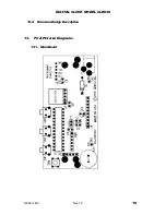
Page 21: ...DIGITAL CLOCK MODEL CLK036 GEKCO INC Rev 1 0 19 12 2 Firmware Design Description 13 PCA Pictorial Diagrams 13 1 Main Board...

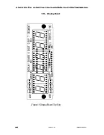
Page 22: ...GEKCO DIGITAL CLOCK P N CLK036 ASSEMBLY OPERATION MANUAL 20 REV 1 0 GEKCO INC 13 2 Display Board Figure 11 Display Board Top Side...

Page 23: ...DIGITAL CLOCK MODEL CLK036 GEKCO INC Rev 1 0 21 Figure 12 Display Board Bottom Side...

Page 24: ...GEKCO DIGITAL CLOCK P N CLK036 ASSEMBLY OPERATION MANUAL 22 REV 1 0 GEKCO INC 14 Schematic Main Board...

Page 25: ...DIGITAL CLOCK MODEL CLK036 GEKCO INC Rev 1 0 23 15 Schematic Display Board...

Page 26: ...GEKCO DIGITAL CLOCK P N CLK036 ASSEMBLY OPERATION MANUAL 24 REV 1 0 GEKCO INC 16 Document Revision History 1 0 3 Dec 18 Initial Release...

Reviews: