background image

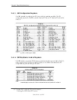
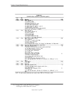
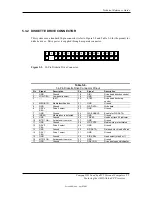
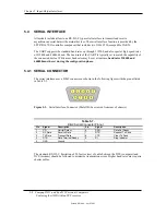
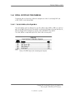
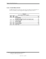
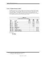
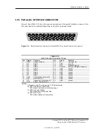
Chapter 5  Input/Output Interfaces


5.5.2  ENHANCED PARALLEL PORT MODE 


In Enhanced Parallel Port (EPP) mode, increased data transfers are possible (up to 2 MB/s) due to 
a hardware protocol that provides automatic address and strobe generation. EPP revisions 1.7 and 
1.9 are both supported. For the parallel interface to be initialized for EPP mode, a negotiation 
phase is entered to detect whether or not the connected peripheral is compatible with EPP mode. If 
compatible, then EPP mode can be used.  In EPP mode, system timing is closely coupled to EPP 
timing. A watchdog timer is used to prevent system lockup.  
 
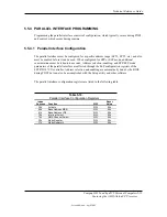
Five additional registers are available in EPP mode to handle 16- and 32-bit CPU accesses with 
the parallel interface.  Address decoding includes address lines A0, A1, and A2. 
 

5.5.3 EXTENDED CAPABILITIES PORT MODE 


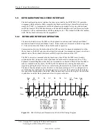
The Extended Capabilities Port (ECP) mode, like EPP, also uses a hardware protocol-based 
design that supports transfers up to 2 MB/s. Automatic generation of addresses and strobes as well 
as Run Length Encoding (RLE) decompression is supported by ECP mode. The ECP mode 
includes a bi-directional FIFO buffer that can be accessed by the CPU using DMA or programmed 
I/O. For the parallel interface to be initialized for ECP mode, a negotiation phase is entered to 
detect whether or not the connected peripheral is compatible with ECP mode. If compatible, then 
ECP mode can be used.        
 
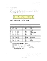
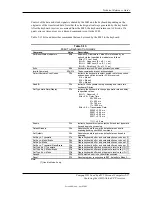
Ten control registers are available in ECP mode to handle transfer operations. In accessing the 
control registers, the base address is determined by address lines A2-A9, with lines A0, A1, and 
A10 defining the offset address of the control register.  Registers used for FIFO operations are 
accessed at their base a 400h (i.e., if configured for LPT1, then 378h + 400h = 778h).  
 
The ECP mode includes several sub-modes as determined by the Extended Control register. Two 
submodes of ECP allow the parallel port to be controlled by software.  In these modes, the FIFO 
is cleared and not used, and DMA and RLE are inhibited.  


5-12

   Compaq D315 and hp d325 Personal Computers            

          Featuring the AMD Athlon XP Processor 


Second Edition – April 2003


Summary of Contents for Compaq D315

Page 1: ...t provides information on the design architecture function and capabilities of the Compaq D315 and the HP d325 Personal Computers This information may be used by engineers technicians administrators or anyone needing detailed information on the products covered Document Part Number 322898 002 ...

Page 2: ......

Page 3: ...in the 8 x 11 inch format The title block below may can be copied and or cut out and placed into a slip or taped onto the binder Compaq D315 and hp d325 Personal Computers featuring the AMD Athlon XP processor and NVidia NForce chipsets TRG ...

Page 4: ......

Page 5: ... the furnishing performance or use of this material The information in this document is provided as is without warranty of any kind including but not limited to the implied warranties of merchantability and fitness for a particular purpose and is subject to change without notice The warranties for HP products are set forth in the express limited warranty statement accompanying such products Nothin...

Page 6: ...Technical Reference Guide Compaq D315 and hp d325 Personal Computers Featuring the AMD Athlon XP Processor Second Edition April 2003 ii ...

Page 7: ... CHAPTER 2 SYSTEM OVERVIEW 2 1 INTRODUCTION 2 1 2 2 FEATURES AND OPTIONS 2 2 2 2 1 STANDARD FEATURES 2 2 2 2 2 OPTIONS 2 3 2 3 MECHANICAL DESIGN 2 4 2 3 1 CABINET LAYOUTS 2 4 2 3 2 CHASSIS LAYOUT 2 6 2 3 3 BOARD LAYOUTS 2 7 2 4 SYSTEM ARCHITECTURE 2 8 2 4 1 AMD ATHLON XP PROCESSOR 2 10 2 4 2 CHIPSET 2 11 2 4 3 SUPPORT COMPONENTS 2 11 2 4 4 SYSTEM MEMORY 2 12 2 4 5 MASS STORAGE 2 12 2 4 6 SERIAL AN...

Page 8: ... 4 9 4 3 1 BUS TRANSACTIONS 4 9 4 3 2 AGP CONNECTOR 4 13 4 4 SYSTEM RESOURCES 4 14 4 4 1 INTERRUPTS 4 14 4 4 2 DIRECT MEMORY ACCESS 4 18 4 5 SYSTEM CLOCK DISTRIBUTION 4 21 4 6 REAL TIME CLOCK AND CONFIGURATION MEMORY 4 22 4 6 1 CLEARING CMOS 4 22 4 6 2 CMOS ARCHIVE AND RESTORE 4 23 4 6 3 STANDARD CMOS LOCATIONS 4 23 4 7 SYSTEM MANAGEMENT 4 24 4 7 1 SECURITY FUNCTIONS 4 24 4 7 2 POWER MANAGEMENT 4 ...

Page 9: ...RFACE OPERATION 5 16 5 6 2 POINTING DEVICE INTERFACE OPERATION 5 18 5 6 3 KEYBOARD POINTING DEVICE INTERFACE PROGRAMMING 5 18 5 6 4 KEYBOARD POINTING DEVICE INTERFACE CONNECTOR 5 21 5 7 UNIVERSAL SERIAL BUS INTERFACE 5 22 5 7 1 USB DATA FORMATS 5 23 5 7 2 USB PROGRAMMING 5 24 5 7 3 USB CONNECTOR 5 25 5 7 4 USB CABLE DATA 5 25 5 8 AUDIO SUBSYSTEM 5 26 5 8 1 FUNCTIONAL ANALYSIS 5 26 5 8 2 AC97 AUDIO...

Page 10: ...N DISTRIBUTION 7 8 7 4 SIGNAL DISTRIBUTION 7 9 CHAPTER 8 SYSTEM BIOS 8 1 INTRODUCTION 8 1 8 2 ROM FLASHING UPGRADING 8 2 8 3 BOOT FUNCTIONS 8 3 8 3 1 BOOT DEVICE ORDER 8 3 8 3 2 NETWORK BOOT F12 SUPPORT 8 3 8 3 3 MEMORY DETECTION AND CONFIGURATION 8 4 8 3 4 BOOT ERROR CODES 8 4 8 4 SETUP UTILITY 8 5 8 5 CLIENT MANAGEMENT FUNCTIONS 8 11 8 5 1 SYSTEM ID AND ROM TYPE 8 13 8 5 2 EDID RETRIEVE 8 13 8 5...

Page 11: ... XX A 8 A 14 HARD DRIVE ERROR MESSAGES 19XX XX A 9 A 15 VIDEO GRAPHICS ERROR MESSAGES 24XX XX A 9 A 16 AUDIO ERROR MESSAGES 3206 XX A 10 A 17 DVD CD ROM ERROR MESSAGES 33XX XX A 10 A 18 NETWORK INTERFACE ERROR MESSAGES 60XX XX A 10 A 19 SCSI INTERFACE ERROR MESSAGES 65XX XX 66XX XX 67XX XX A 11 A 20 POINTING DEVICE INTERFACE ERROR MESSAGES 8601 XX A 11 APPENDIX B ASCII CHARACTER SET B 1 INTRODUCTI...

Page 12: ...WAKE UP FUNCTIONS D 3 D 2 3 IPSEC FUNCTION D 4 D 3 POWER MANAGEMENT SUPPORT D 5 D 3 1 APM ENVIRONMENT D 5 D 3 2 ACPI ENVIRONMENT D 5 D 4 ADAPTER PROGRAMMING D 6 D 4 1 CONFIGURATION D 6 D 4 2 CONTROL D 6 D 5 NETWORK CONNECTOR D 7 D 6 ADAPTER SPECIFICATIONS D 7 Compaq D315 and hp d325 Personal Computers Featuring the AMD Athlon XP Processor Second Edition April 2003 viii ...

Page 13: ...N PRIMARY IDE CONNECTOR ON SYSTEM BOARD 5 3 FIGURE 5 2 34 PIN DISKETTE DRIVE CONNECTOR 5 7 FIGURE 5 3 SERIAL INTERFACE CONNECTOR MALE DB 9 AS VIEWED FROM REAR OF CHASSIS 5 8 FIGURE 5 4 PARALLEL INTERFACE CONNECTOR FEMALE DB 25 AS VIEWED FROM REAR OF CHASSIS 5 15 FIGURE 5 5 8042 TO KEYBOARD TRANSMISSION OF CODE EDH TIMING DIAGRAM 5 16 FIGURE 5 6 KEYBOARD OR POINTING DEVICE INTERFACE CONNECTOR 5 21 ...

Page 14: ...DOWS 102W KEY KEYBOARD KEY POSITIONS C 6 FIGURE C 7 7 BUTTON EASY ACCESS KEYBOARD LAYOUT C 7 FIGURE C 8 8 BUTTON EASY ACCESS KEYBOARD LAYOUT C 7 FIGURE C 9 PS 2 KEYBOARD CABLE CONNECTOR MALE C 16 FIGURE C 10 USB KEYBOARD CABLE CONNECTOR MALE C 16 FIGURE D 1 INTEL PRO 100 OR PRO 100 S MANAGEMENT ADAPTER CARD LAYOUT D 1 FIGURE D 2 INTEL PRP 100 MANAGEMENT ADAPTER BLOCK DIAGRAM D 2 FIGURE D 3 ETHERNE...

Page 15: ...ONFIGURATION MEMORY CMOS MAP 4 23 TABLE 4 12 SYSTEM BOOT ROM FLASH STATUS LED INDICATIONS 4 26 TABLE 4 13 SYSTEM OPERATIONAL STATUS LED INDICATION 4 27 TABLE 4 14 SYSTEM I O MAP 4 30 TABLE 4 15 LPC47B367 I O CONTROLLER REGISTERS 4 31 TABLE 5 1 IDE PCI CONFIGURATION REGISTERS 5 2 TABLE 5 2 IDE BUS MASTER CONTROL REGISTERS 5 2 TABLE 5 3 40 PIN PRIMARY IDE CONNECTOR PINOUT 5 3 TABLE 5 4 DISKETTE DRIV...

Page 16: ...ETUP UTILITY FUNCTIONS 8 5 TABLE 8 4 CLIENT MANAGEMENT FUNCTIONS INT15 8 11 TABLE A 1 BEEP KEYBOARD LED CODES A 1 TABLE A 2 POWER ON SELF TEST POST MESSAGES A 2 TABLE A 3 SYSTEM ERROR MESSAGES A 3 TABLE A 4 MEMORY ERROR MESSAGES A 4 TABLE A 5 KEYBOARD ERROR MESSAGES A 4 TABLE A 6 PRINTER ERROR MESSAGES A 5 TABLE A 7 VIDEO GRAPHICS ERROR MESSAGES A 5 TABLE A 8 DISKETTE DRIVE ERROR MESSAGES A 6 TABL...

Page 17: ...NE VIEWING Online viewing allows for quick navigating and convenient searching through the document A color monitor will also allow the user to view the color shading used to highlight differential data A softcopy of the latest edition of this guide is available for downloading in pdf file format at the URL listed below http www3 compaq com support home selectproduct asp destination reflib pid 1 V...

Page 18: ...CONVENTION Two model numbering conventions one for Compaq one for HP are used for the systems covered in this guide 1 3 1 COMPAQ MODEL NUMBERING CONVENTION The model numbering convention for Compaq systems is as follows XXX XNN NN N NNNx Removable storage b CD CDRW c CD d DVD r CDRW z ZIP Memory in MB OS type 2 Windows 2000 6 Dual install Windows NT 4 0 or 2000 8 Windows 98SE P Dual install Window...

Page 19: ...R333 dual channel F DDR400 single channel G DDR400 dual channel Memory Amount 3 digits MB 2 digits GB Removable storage c CD ROM d DVD ROM q DVD RW r CDRW w DVD CDRW combo z ZIP drive y drive key n no diskette drive x no removable storage blank diskette 2 nd Hard drive if installed Hard drive speed a 5400 rpm b 7200 rpm Hard drive size in GB Processor speed 2 or 3 digits in GHz Processor type A AM...

Page 20: ...ions in discussing the microprocessor s CPU internal registers Registers that are accessed through programmable I O using an indexing scheme are indicated using the following format 03C5 17h Index port Data port In the example above register 03C5 17h is accessed by writing the index port value 17h to the index address 03C4h followed by a write to or a read from port 03C5h 1 5 4 BIT NOTATION AND BY...

Page 21: ...et interface extensions AVI audio video interleaved AVGA Advanced VGA AWG American Wire Gauge specification BAT Basic assurance test BCD binary coded decimal BIOS basic input output system bis second new revision BNC Bayonet Neill Concelman connector type bps or b s bits per second BSP Bootstrap processor BTO Built to order CAS column address strobe CD compact disk CD ROM compact disk read only me...

Page 22: ...el port EIDE enhanced IDE ESCD Extended System Configuration Data format EV Environmental Variable data ExCA Exchangeable Card Architecture FIFO first in first out FL flag register FM frequency modulation FPM fast page mode RAM type FPU Floating point unit numeric or math coprocessor FPS Frames per second ft Foot feet GB gigabyte GMCH Graphics memory controller hub GND ground GPIO general purpose ...

Page 23: ...ssor MMX multimedia extensions MPEG Motion Picture Experts Group ms millisecond MSb MSB most significant bit most significant byte mux multiplex MVA motion video acceleration MVW motion video window n variable parameter value NIC network interface card controller NiMH nickel metal hydride NMI non maskable interrupt NRZI Non return to zero inverted ns nanosecond NT nested task flag NTSC National Te...

Page 24: ...SDR Singles data rate memory SDRAM Synchronous Dynamic RAM SEC Single Edge Connector SECAM sequential colour avec memoire sequential color with memory SF sign flag SGRAM Synchronous Graphics RAM SIMD Single instruction multiple data SIMM single in line memory module SMART Self Monitor Analysis Report Technology SMI system management interrupt SMM system management mode SMRAM system management RAM ...

Page 25: ...stor logic TV television TX transmit UART universal asynchronous receiver transmitter UDMA Ultra DMA URL Uniform resource locator us µs microsecond USB Universal Serial Bus UTP unshielded twisted pair V volt VAC Volts alternating current VDC Volts direct current VESA Video Electronic Standards Association VGA video graphics adapter VLSI very large scale integration VRAM Video RAM W watt WOL Wake O...

Page 26: ...Chapter 1 Introduction Compaq D315 and hp d325 Personal Computers Featuring the AMD Athlon XP Processor Second Edition April 2003 1 10 This page is intentionally blank ...

Page 27: ...along with industry compatibility These models feature an architecture incorporating the PCI bus All models are easily upgradeable and expandable to keep pace with the needs of the office enterprise hp d325 Compaq D315 Figure 2 1 Compaq D315 and hp d325 Personal Computers This chapter includes the following topics Features and options 2 2 page 2 2 Mechanical design 2 3 page 2 4 System architecture...

Page 28: ...iant Security features including Flash ROM Boot Block Diskette drive disable boot disable write protect Power on password Administrator password Serial parallel port disable PS 2 Compaq Easy Access keyboard w Windows support PS 2 Compaq Scroll Mouse 220 watt Power Supply Available with Windows XP Home XP Professional or Mandrake Linux 8 2 Table 2 1 lists the differences between the Compaq D315 and...

Page 29: ...ed non ECC PC2700 128 MB DDR DIMM unbuffered non ECC PC2700 256 MB DDR DIMM unbuffered non ECC PC2700 512 MB DDR DIMM unbuffered non ECC Hard drives controllers 20 40 60 or 80 GB UATA 100 hard drive 32 GB Wide Ultra3 SCSI hard drive Removeable media drives 16x 10x 40x CD RW drive 10x 40x Max DVD ROM drive LS 120 Super Disk drive PCI DXR DVD Decoder kit Graphics Monitors Compaq P700 17 CRT Compaq P...

Page 30: ...se systems refer to the applicable Service Reference Guide Service personnel should review training materials also available on these products 2 3 1 CABINET LAYOUTS 2 3 1 1 Front Views 8 9 7 12 11 10 6 5 4 2 3 1 8 9 7 12 11 10 6 5 4 2 3 1 Compaq D315 hp d325 Item Description 1 CD ROM drive headphone jack 2 CD ROM drive volume control 3 CD ROM drive activity LED 4 CD ROM drive open close button 5 1...

Page 31: ...tion 1 AC voltage switch 7 VGA monitor connector 2 AC power connector 8 Audio microphone in jack 3 Mouse connector 9 Audio line input jack 4 Keyboard connector 10 Audio line output jack 5 Serial connector 11 Network interface connector 6 Parallel connector 12 USB ports 4 Figure 2 3 Cabinet Layout Rear Views Compaq D315 and hp d325 Personal Computers Featuring the AMD Athlon XP Processor Second Edi...

Page 32: ... or hp d325 personal computers Front Back Power Supply Chassis Fan AGP Slot NIC Card 1 in PCI Slot 1 PCI Slot 2 PCI Slot 3 Externally Accessible Drive Bays Processor Heat Sink Fan Assembly Internal Drive Bays Front Panel Audio USB board NOTES LEGEND 1 If present D315 model board mounted horizontally d325 model board mounted veritically Figure 2 4 Chassis Layout Left Side View Compaq D315 and hp d3...

Page 33: ...ector 26 AGP slot 8 USB ports 2 27 Safe mode jumper 9 Top Mouse port bottom keyboard port 28 PCI bus expansion connector 1 10 CD audio connector 29 Auxiliary audio connector 11 Processor power 30 Serial port COM1 conenc tor 12 Processor socket 31 MultiBay connector 13 Processor fan connector 32 Hood sense connector 14 Fan ground control 33 Hood lock connector 15 Fan power control 34 BIOS boot bloc...

Page 34: ...supporting up to four ATA100 storage devices Six USB ports AC link interface servicing the audio controller PCI bus controller supporting up to three 32 bit 33 MHz PCI expansion devices LPC bus interface serving the BIOS ROM and super I O component Table 2 1 lists the architectural differences between the D315 and d325 models Table 2 2 Feature Difference Matrix Table 2 2 Architectural Difference M...

Page 35: ...lel I F Serial I F BIOS ROM AGP Slot Monitor RGB CD Audio Beep Audio AC 97 Link Bus Audio Subsystem FSB Memory Bus DDR SDRAM Athlon XP Processor PCI Slot 1 PCI Slot 2 PCI Slot 3 Hyper Transport Link Bus NForce Chipset ATA100 Hard Drive 33 MHz 32 Bit PCI Bus Sec IDE Cntlr Power Supply USB Cntlrs Pri IDE Cntlr South Bridge Figure 2 6 System Architecture Block Diagram Compaq D315 and hp d325 Personal...

Page 36: ...U core to process more instructions in a given clock cycle than other x86 type processors Optimized for the Windows XP operating systems the Athlon XP processor is also compatible with all earlier Windows operating systems Windows 2000 ME and 98 These systems use the Socket A method of processor mounting as shown in Figure 2 7 Heat Sink Fan Assembly OPGA2 Package Socket A Fan Power Cable Heat Sink...

Page 37: ...es Yes Yes NOTE Unless otherwise indicated all functions are common to both chipsets 2 4 3 SUPPORT COMPONENTS Input output functions not provided by the chipset are handled by other support components Some of these components also provide housekeeping and various other functions as well Table 2 4 shows the functions provided by the support components Table 2 4 Support Component Functions Table 2 4...

Page 38: ...r two drives for a total of four IDE devices although the form factor will determine the actual number of drive spaces available 2 4 6 SERIAL AND PARALLEL INTERFACES This system includes one serial port and a parallel port accessible at the rear of the chassis The serial interface is RS 232 C 16550 compatible and supports standard baud rates up to 115 200 as well as two high speed baud rates of 23...

Page 39: ...essing unit The system may be upgraded adding a separate AGP card to replace the integrated graphic controller Table 2 5 lists the key specifications of the standard graphics subsystems employed in these systems Table 2 5 Standard Graphics Subsystem Comparison Table 2 5 Standard Graphics Support Comparison D315 d325 Bus Type AGP 4X AGP 8X Graphics processing unit GeForce 2 MX GeForce 4 MX DAC Spee...

Page 40: ... Parameter Operating Nonoperating Ambient Air Temperature 50 o to 95 o F 10 o to 35 o C max rate of change 10 C Hr 24 o to 140 o F 30 o to 60 o C max rate of change 20 C Hr Shock w o damage 5 Gs 1 20 Gs 1 Vibration 0 000215 G 2 Hz 10 300 Hz 0 0005 G 2 Hz 10 500 Hz Humidity 10 90 Rh 28 o C max wet bulb temperature 5 95 Rh 38 7 o C max wet bulb temperature Maximum Altitude 10 000 ft 3048 m 2 30 000 ...

Page 41: ...another system unit Table 2 9 Diskette Drive Specifications Table 2 9 Diskette Drive Specifications Compaq SP 278644 001 Parameter Measurement Media Type 3 5 in 1 44 MB 720 KB diskette Height 1 3 bay 1 in Bytes per Sector 512 Sectors per Track High Density Low Density 18 9 Tracks per Side High Density Low Density 80 80 Read Write Heads 2 Average Access Time Track to Track high low Average high low...

Page 42: ...um 1 6 um Laser Beam Divergence Output Power Type Wave Length 53 5 1 5 53 6 0 14 mW GaAs 790 25 nm 53 5 1 5 53 6 0 14 mW GaAs 790 25 nm Average Access Time Random Full Stroke 100 ms 150 ms 120 ms 200 ms Audio Output Level 0 7 Vrms 0 7 Vrms Cache Buffer 128 KB 128 KB Table 2 11 Hard Drive Specifications Table 2 11 Hard Drive Specifications Parameter 20 0 GB 20 0 GB 40 0 GB 40 0 GB Part Number 24940...

Page 43: ...n chapter 6 HT I F Memory Cntlr FSB I F IGP GPU AGP I F DIMM In Socket Memory Bus 1 Cntl 64 Bit FSB Athlon XP Processor DIMM Socket System Memory XMM1 XMM2 1 D315 64 bit d325 128 bit max Figure 3 1 Processor Memory Subsystem Architecture This chapter includes the following topics AMD Athlon XP processor 3 2 page 3 2 Memory subsystem 3 3 page 3 5 Subsystem configuration 3 4 page 3 8 Compaq D315 and...

Page 44: ...fer for data and instruction addresses Large full speed 384 KB cache 128 KB L1 cache and 256 KB L2 cache Enhanced Floating Point Processor Executes all x87 math co processor MMX SSE and 3DNow instructions Advanced dynamic branch prediction The Athlon XP processor is backward compatible with software written for most x86 type processors such as the AMD Athlon 4 AMD Duron and Intel Pentium processor...

Page 45: ...60 3 W 61 3 W Model 6 2100 1733 MHz 1 75 VDC 41 1 A 72 0 W Model 8 2100 1733 MHz 1 60 VDC 38 8 A 61 1 W Model 8 2200 1800 MHz 1 60 VDC 41 2 A 39 3 A 67 9 W 62 8 W Model 8 2400 2000 MHz 1 65 VDC 41 4 A 68 3 W Model 8 2600 2133 MHz 2083 MHz 1 65 VDC 41 4 A 68 3 W Model 8 2800 2083 MHz 1 65 VDC 41 4 A 68 3 W Model 8 3000 2167 MHz 1 65 VDC 45 0 A 74 3 W Figure 3 2 AMD Athlon XP Processor Internal Arch...

Page 46: ...essor that exceeds a particular model s capability may result in equipment failure and or damage NOTE These systems ship with Athlon XP processors but do support Duron processors as well The heat sink is specially designed provide maximum heat transfer from the processor component CAUTION Attachment of the heat sink to the processor is critical on these systems Improper attachment of the heat sink...

Page 47: ...est technology level supported 512 Mb 1024 Mb Maximum amount supported 1 GB 2 GB The SPD format as supported in this system SPD rev 1 is shown in Table 3 1 All DIMMs must yield a value of 07h indicating DDR memory in SPD byte 02 i e only DDR DIMMs are supported in these systems The memory subsystem is controlled by the memory controller integrated into the IGP component of the NVidia NForce chipse...

Page 48: ...ported 4 127 Reserved 19 CS Latency 4 128 131 Compaq header CPQ1 9 20 Write Latency 4 132 Header checksum 9 21 DIMM Attributes 133 145 Unit serial number 9 10 22 Memory Device Attributes 146 DIMM ID 9 11 23 Min CLK Cycle Time at CL X 1 7 147 Checksum 9 24 Max Acc Time From CLK CL X 1 7 Reserved 9 NOTES 1 Programmed as 128 bytes by the DIMM OEM 2 Must be programmed to 256 bytes 3 High order bit def...

Page 49: ...Mem Area 128 KB System BIOS Area 128 KB max 2 Graphics SMRAM RAM 128 KB FFFF FFFFh FFE0 0000h FFDF FFFFh Host PCI Memory Expansion 496 MB High BIOS Area 2 MB 1 16 MB 1 MB 640 KB 512 KB NOTE All locations in memory are cacheable Base memory is always mapped to DRAM The next 128 KB fixed memory area can through the north bridge be mapped to DRAM or to PCI space Graphics RAM area is mapped to PCI or ...

Page 50: ...Chapter 3 Processor Memory Subsystem Compaq D315 and hp d325 Personal Computers Featuring the AMD Athlon XP Processor Second Edition April 2003 3 8 This page is intentionally blank ...

Page 51: ...clock and configuration memory 4 6 page 4 21 System management 4 7 page 4 23 Register map and miscellaneous functions 4 8 page 4 29 This chapter covers functions provided by off the shelf chipsets and therefore describes only basic aspects of these functions as well as information unique to the systems covered in this guide For detailed information on specific components refer to the applicable ma...

Page 52: ...ontain one or more functions In the standard configuration these systems use a hierarchy of three PCI buses Figure 4 1 The PCI bus 0 is internal to the chipset components and is not physically accessible The AGP bus that services the AGP slot is designated as PCI bus 1 All PCI slots reside on PCI bus 2 Network Interface Function USB Cntlr b Function PCI Bus 2 PCI Connector 1 PCI Connector 2 PCI Co...

Page 53: ...dressing assumed to increment accordingly four bytes at a time 4 2 1 2 Configuration Cycles Devices on the PCI bus must comply with PCI protocol that allows configuration of that device by software In this system configuration mechanism 1 as described in the PCI Local Bus specification Rev 2 2 is employed This method uses two 32 bit registers for initiating a configuration cycle for accessing the ...

Page 54: ...ts and slots residing on a PCI bus Table 4 1 PCI Device Configuration Access Table 4 1 PCI Component Configuration Access PCI Component Function PCI Bus Device Function Device ID 4 IDSEL Wired to 4 IGP CPU Host Bridge Memory Configuration Memory Addr Trans Cntrl Miscellaneous Control AGP Host Graphics processing unit 1 0 0 0 0 0 1 0 0 0 0 30 0 0 1 2 3 0 0 01A4h 01E0h 01Ach 01EBh 01ADh 01EEh 01AAh ...

Page 55: ...1 Command Revision ID Line Size Class Code Hdr Type Status Not required 00h Register Index Base Address Registers BIST Min Lat Int Line Lat Timer Device Specific Area Card Bus CIS Pointer Reserved Min GNT Int Pin Reserved Expansion ROM Base Address Subsystem ID Subsystem Vendor ID Device ID Status Hdr Type Class Code Vendor ID 0 7 8 15 16 23 24 31 Command Revision ID Line Size 3Ch 40h 38h FCh 2Ch ...

Page 56: ...e bus a request is not needed and the device can simply assert FRAME and conduct the transaction Table 4 2 shows the grant and request signals assignments for the devices on the PCI bus Table 4 2 PCI Bus Mastering Devices Table 4 2 PCI Bus Mastering Devices REQ GNT Line Device REQ0 GNT0 PCI Connector Slot 1 REQ1 GNT1 PCI Connector Slot 2 REQ2 GNT2 PCI Connector Slot 3 GREQ GGNT AGP Slot NOTE PCI b...

Page 57: ...orted by the chipset and allows compliant PCI and AGP peripherals to initiate the power management routine 4 2 6 PCI SUB BUSSES The chipset implements two data busses that are supplementary in operation to the PCI bus 4 2 6 1 Hyper Transfer Link Bus The NVidia NForce chipset implements a Hyper Transfer Link bus between the IGP and the MCP components This bus operates at 800 MHz and is transparent ...

Page 58: ... GND GND 43 3 3 VDC PAR 74 AD55 AD54 13 GND GND 44 C BE1 AD15 75 AD53 5 VDC 14 RSVD 3 3 AUX 45 AD14 3 3 VDC 76 GND AD52 15 GND RST 46 GND AD13 77 AD51 AD50 16 CLK 5 VDC 47 AD12 AD11 78 AD49 GND 17 GND GNT 48 AD10 GND 79 5 VDC AD48 18 REQ GND 49 GND AD09 80 AD47 AD46 19 5 VDC PME 50 Key Key 81 AD45 GND 20 AD31 AD30 51 Key Key 82 GND AD44 21 AD29 3 3 VDC 52 AD08 C BE0 83 AD43 AD42 22 GND AD28 53 AD0...

Page 59: ... PCI bus controller Key differences between the AGP interface and the PCI interface are as follows Address phase and associated data transfer phase are disconnected transactions Addressing and data transferring occur as contiguous actions on the PCI bus On the AGP bus a request for data and the transfer of data may be separated by other operations Commands on the AGP bus specify system memory acce...

Page 60: ...ves at least eight bytes requiring the 32 AD lines to handle at least two transfers per request The AGP v 2 0 specification used on D315 models supports three transfer rates 1X 2X and 4X The AGP v3 0 specification used on d325 models supports a fourth transfer rate 8X Regardless of the rate used the speed of the bus clock is constant at 66 MHz The following subsections describe how the use of addi...

Page 61: ...D_STBx CLK GNT TRDY T6 T7 T5 T4 T3 T2 T1 Figure 4 6 AGP 2X Data Transfer Peak Transfer Rate 532 MB s AGP 4X Transfers The AGP 4X transfer rate allows sixteen bytes of data to be transferred in one clock cycle As in 2X transfers the 66 MHz CLK signal is used only for qualifying control signals while strobe signals are used to latch each 4 byte transfer on the AD lines As shown in Figure 4 7 4 byte ...

Page 62: ... 4 byte transfer on the AD lines As shown in Figure 4 8 4 byte block DnA is latched by the falling edge of AD_STBx while DnB is latched by the falling edge of AD_STBx The signal level for AGP 8X transfers can be 0 8 or 1 5 VDC Figure 4 8 AGP 8X Data Transfer Peak Transfer Rate 2128 MB s D1A D2A D1B D3A D3B D4A D4B D2B TRDY AD_STBF CLK AD AD_STBS T2 T1 1 Data Latched st Final Data Latched Compaq D3...

Page 63: ...AD24 PAD25 52 VDDQ VDDQ 09 VDD3 VDD3 31 GND GND 53 PAD13 PAD14 10 ST1 ST0 32 AD_STB1 AD_STB1 54 PAD11 PAD12 11 NC ST2 33 CBE3 PAD23 55 GND GND 12 PIPE RBF 34 VDDQ VDDQ 56 PAD09 PAD10 13 GND GND 35 PAD22 PAD21 57 CBE0 PAD08 14 WBF NC 36 PAD20 PAD19 58 VDDQ VDDQ 15 SBA1 SBA0 37 GND GND 59 AD_STB0 AD_STB0 16 VDD3 VDD3 38 PAD18 PAD17 60 PAD06 PAD07 17 SBA3 SBA2 39 PAD16 CBE2 61 GND GND 18 SB_STB SB_ST...

Page 64: ...o get the attention of the microprocessor Peripheral functions produce a unique INTA H PCI or IRQ0 15 ISA signal that is routed to interrupt processing logic that asserts the interrupt INTR input to the microprocessor The microprocessor halts execution to determine the source of the interrupt and then services the peripheral as appropriate Figure 4 9 shows the routing of PCI and ISA interrupts Mos...

Page 65: ...al port COM1 13 IRQ5 Network interface controller 14 IRQ6 Diskette drive controller 15 IRQ7 Parallel port LPT1 IRQ2 NOT AVAILABLE Cascade from interrupt controller 2 APIC Mode The Advanced Programmable Interrupt Controller APIC mode provides enhanced interrupt processing with the following advantages Eliminates the processor s interrupt acknowledge cycle by using a separate APIC bus Programmable i...

Page 66: ...nitialization and operation of the interrupt control registers follows standard AT type protocol 4 4 1 2 Non Maskable Interrupts Non maskable interrupts cannot be masked inhibited within the microprocessor itself but may be maskable by software using logic external to the microprocessor There are two non maskable interrupt signals the NMI and the SMI These signals have service priority over all ma...

Page 67: ... the active NMI has been processed status bits 7 or 6 are cleared by pulsing bits 2 or 3 respectively The NMI Enable Register 070h 7 is used to enable disable the NMI signal Writing 80h to this register masks generation of the NMI Note that the lower six bits of register at I O port 70h affect RTC operation and should be considered when changing NMI generation status SMI Generation The SMI System ...

Page 68: ...ID Controller 1 byte transfers 0 1 2 3 Spare Audio subsystem Diskette drive Parallel port Controller 2 word transfers 4 5 6 7 Cascade for controller 1 Spare Spare Spare All channels in DMA controller 1 operate at a higher priority than those in controller 2 Note that channel 4 is not available for use other than its cascading function for controller 1 The DMA controller 2 can transfer words only o...

Page 69: ...emory page register for the refresh channel must be programmed with 00h for proper operation The memory address is derived as follows 24 Bit Address Controller 1 Byte Transfers 8 Bit Page Register 8 Bit DMA Controller A23 A16 A15 A00 24 Bit Address Controller 2 Word Transfers 8 Bit Page Register 16 Bit DMA Controller A23 A17 A16 A01 A00 0 Note that address line A16 from the DMA memory page registe...

Page 70: ...ller Table 4 9 DMA Controller Registers Table 4 9 DMA Controller Registers Register Controller 1 Controller 2 R W Status 008h 0D0h R Command 008h 0D0h W Mode 00Bh 0D6h W Write Single Mask Bit 00Ah 0D4h W Write All Mask Bits 00Fh 0DEh W Software DRQx Request 009h 0D2h W Base and Current Address Ch 0 000h 0C0h W Current Address Ch 0 000h 0C0h R Base and Current Word Count Ch 0 001h 0C2h W Current Wo...

Page 71: ...rt Bus clock 133 166 MHz 1 IGP Processor DIMM sockets 66 MHz IGP AGP slot 33 MHz IGP APIC clock 32 768 MHz Crystal MCP super I O 25 MHz Crystal NIC PHY 25 MHz NIC PHY MCP 24 576 MHz Crystal Audio codec 16 MHz IGP APIC clock 14 31818 MHz Crystal MCP 14 31818 MHz MCP Clock buffer 14 31818 MHz Clock buffer IGP super I O 12 288 MHz Audio codec AC link clock NOTE 1 D315 d325 These systems uses the spre...

Page 72: ... CMOS Figure 4 11 Configuration Memory Map A lithium 3 VDC battery is used for maintaining the RTC and configuration memory while the system is powered down The battery is located in a battery holder on the system board and has a life expectancy of about three years When the battery has expired it is replaced with a Renata CR2032 or equivalent 3 VDC lithium battery 4 6 1 CLEARING CMOS The contents...

Page 73: ...rd ID 0Eh Diagnostic status 25h System architecture data 0Fh System reset code 26h Auxiliary peripheral configuration 10h Diskette drive type 27h Speed control external drive 11h Reserved 28h Expanded base mem size IRQ12 12h Hard drive type 29h Miscellaneous configuration 13h Security functions 2Ah Hard drive timeout 14h Equipment installed 2Bh System inactivity timeout 15h Base memory size low by...

Page 74: ...on and described below or the entire CMOS be cleared refer to section 4 6 To clear only the password use the following procedure 1 Turn off the system and disconnect the AC power cord from the outlet and or system unit 2 Remove the cover hood as described in the appropriate User Guide or Service Reference Guide Insure that any system board LEDs are off not illuminated 3 Locate the password clear h...

Page 75: ... the Setup utility to guard against unauthorized access to a system In addition the ability to write to or boot from a removable media drive such as the diskette drive may be enabled through the Setup utility The disabling of the serial parallel and diskette interfaces are a function of the LPC47B367 I O controller The USB ports are controlled through the MCP Compaq D315 and hp d325 Personal Compu...

Page 76: ...e valid only for PS 2 type keyboards A USB keyboard will not provide LED status for the listed events although audible beep indications will occur Table 4 12 System Boot ROM Flash Status LED Indications Table 4 12 System Boot ROM Flash Status LED Indications Event NUM Lock LED CAPs Lock LED Scroll Lock LED System memory failure 1 Blinking Off Off Graphics controller failure 2 Off Blinking Off Syst...

Page 77: ... in six seconds followed by two second pause 5 Sequence blinks red seven times in seven seconds followed by two second pause 6 Sequence blinks red eight times in eight seconds followed by two second pause 4 7 4 THERMAL SENSING AND COOLING These systems feature variable speed fans that are controlled through temperature sensing logic on the system board and or in the power supply Typical cooling co...

Page 78: ...ry be inadequate or fail it may be desirable to have the fans driven by a constant 12 VDC by configuring both FAN_SEL jumpers to pins 1 and 2 Note that the power supply assembly fan operates independently of the CPU and chassis fans CAUTION Both FAN_SELn jumpers must have the same configuration jumpers on the same pins Different jumper settings one jumper on pins 1 and 2 and the other jumper on pi...

Page 79: ... than normal level during the initial start up to protect against the possibility of an incorrectly installed heat sink If during the boot period the processor s temperature reaches 100 C the hardware Monitor will assert the Therm signal causing the I O Controller to de assert the PS On signal which will shut down the power supply If the processor does not reach 100 C during the boot sequence the ...

Page 80: ...active only if standard I O space is enabled for primary drive 01F0 01F7h IDE Controller 1 active only if standard I O space is enabled for secondary drive 0278 027Fh Parallel Port LPT2 02E8 02EFh Serial Port COM4 02F8 02FFh Serial Port COM2 0370 0377h Diskette Drive Controller Secondary Address 0376h IDE Controller 2 active only if standard I O space is enabled for primary drive 0378 037Fh Parall...

Page 81: ...05h Serial I F UART 2 Port B 06h Reserved 07h Keyboard I F 08h Reserved 09h Reserved 0Ah Runtime Registers GPIO Config 0Bh SMBus Configuration 00h 20h Super I O ID Register SID 56h 21h Revision 22h Logical Device Power Control 00h 23h Logical Device Power Management 00h 24h PLL Oscillator Control 04h 25h Reserved 26h Configuration Address Low Byte 27h Configuration Address High Byte 28 2Fh Reserve...

Page 82: ...rror d325 only See note 5 Off 6 System board failure d325 only See note 6 Off 7 Invalid ROM checksum d325 only See note 7 Off 8 System off Off Off None NOTES 1 Red during flash then blinks green 1 Hz when user can reboot 2 Repetitive sequence of 2 red blinks 1 Hz followed by 2 second pause 3 Repetitive sequence of four red blinks 1 Hz followed by 2 second pause 4 Repetitive sequence of five red bl...

Page 83: ...e consists of primary and secondary controllers integrated into the south bridge component of the chipset Two 40 pin IDE connectors one for each controller are included on the system board Each controller can be configured independently for the following modes of operation Programmed I O PIO mode CPU controls drive transactions through standard I O mapped registers of the IDE drive 8237 DMA mode C...

Page 84: ...Bh Sec CMD I O Base Addr 1d 58 59h IDE Timing A8A8h 1C 1Fh Sec Cntrl I O Base Addr 1d 5A 5Bh IDE Timing A8A8h 20h Bus Mstr I O Base Addr 1d 5Ch IDE Cycle Addr Timing 00FFh 2Ch Subsystem Vendor ID 0000h 5Dh IDD Cycle Addr Timing FFFFh 2Eh Subsystem ID 0000h 60h UDMA Mode Selection 0s 34h Capabilities Pointer 44h NOTES 1 D315 01BCh d325 0065h 5 2 1 2 IDE Bus Master Control Registers The IDE interfac...

Page 85: ... 9 DD4 Data Bit 4 29 DAK DMA Acknowledge 10 DD11 Data Bit 11 30 GND Ground 11 DD3 Data Bit 3 31 IRQn Interrupt Request 4 12 DD12 Data Bit 12 32 IO16 16 bit I O 13 DD2 Data Bit 2 33 DA1 Address 1 14 DD13 Data Bit 13 34 DSKPDIAG Pass Diagnostics 15 DD1 Data Bit 1 35 DA0 Address 0 16 DD14 Data Bit 14 36 DA2 Address 2 17 DD0 Data Bit 0 37 CS0 Chip Select 18 DD15 Data Bit 15 38 CS1 Chip Select 19 GND G...

Page 86: ... phase consists of several bytes written in series from the CPU to the data register 3F5h 375h The first byte identifies the command and the remaining bytes define the parameters of the command The Main Status register 3F4h 374h provides data flow control for the diskette drive controller and must be polled between each byte transfer during the Command phase The Execution phase starts as soon as t...

Page 87: ...o I O register 2Eh 4 Write 01h to I O register 2Fh this activates the interface Writing AAh to 2Eh deactivates the configuration phase The diskette drive I F configuration registers are listed in the following table Table 5 4 Diskette Drive Controller Configuration Registers Table 5 4 Diskette Drive Interface Configuration Registers Index Address Function R W Reset Value 30h Activate R W 01h 60 61...

Page 88: ...ive R W 3F3h 373h Tape Drive Register available for compatibility R W 3F4h 374h Main Status Register MSR 7 Request for master host can transfer data active high 6 Transfer direction 0 write 1 read 5 non DMA execution active high 4 Command busy active high 3 2 Reserved 1 0 Drive 1 2 busy active high Data Rate Select Register DRSR 7 Software reset active high 6 Low power mode enable active high 5 Re...

Page 89: ...20 STEP Drive head track step control 4 MEDIA ID Media identification 21 GND Ground 5 GND Ground 22 WR DATA Write data 6 DRV 4 SEL Drive 4 select 23 GND Ground 7 GND Ground 24 WR ENABLE Enable for WR DATA 8 INDEX Media index is detected 25 GND Ground 9 GND Ground 26 TRK 00 Heads at track 00 indicator 10 MTR 1 ON Activates drive motor 27 GND Ground 11 GND Ground 28 WR PRTK Media write protect statu...

Page 90: ...phase 5 4 1 SERIAL CONNECTOR The serial interface uses a DB 9 connector as shown in the following figure with the pinout listed in Table 5 5 Figure 5 3 Serial Interface Connector Male DB 9 as viewed from rear of chassis Table 5 7 DB 9 Serial Connector Pinout Table 5 7 DB 9 Serial Connector Pinout Pin Signal Description Pin Signal Description 1 CD Carrier Detect 6 DSR Data Set Ready 2 RX Data Recei...

Page 91: ...rial interface are affected through the PnP configuration registers of the LPC47B367 I O controller The serial interface configuration registers are listed in the following table Table 5 8 Serial Interface Configuration Registers Table 5 8 Serial Interface Configuration Registers Index Address Function R W 30h Activate R W 60h Base Address MSB R W 61h Base Address LSB R W 70h Interrupt Select R W ...

Page 92: ...OM2 Addr Register R W 3F8h 2F8h Receive Data Buffer Transmit Data Buffer Baud Rate Divisor Register 0 when bit 7 of Line Control Reg Is set R W W 3F9h 2F9h Baud Rate Divisor Register 1 when bit 7 of Line Control Reg Is set Interrupt Enable Register W R W 3FAh 2FAh Interrupt ID Register FIFO Control Register R W 3FBh 2FBh Line Control Register R W 3FCh 2FCh Modem Control Register R W 3FDh 2FDh Line...

Page 93: ...f the parallel port yields the last data byte that was written The following steps define the standard procedure for communicating with a printing device 1 The system checks the Printer Status register If the Busy Paper Out or Printer Fault signals are indicated as being active the system either waits for a status change or generates an error message 2 The system sends a byte of data to the Printe...

Page 94: ... generation of addresses and strobes as well as Run Length Encoding RLE decompression is supported by ECP mode The ECP mode includes a bi directional FIFO buffer that can be accessed by the CPU using DMA or programmed I O For the parallel interface to be initialized for ECP mode a negotiation phase is entered to detect whether or not the connected peripheral is compatible with ECP mode If compatib...

Page 95: ...d through the PnP configuration registers of the LPC47B367 I O controller Address selection and enabling are automatically done by the BIOS during POST but can also be accomplished with the Setup utility and other software The parallel interface configuration registers are listed in the following table Table 5 10 Parallel Interface Configuration Registers Table 5 10 Parallel Interface Configuratio...

Page 96: ...ers Table 5 11 Parallel Interface Control Registers I O Address Register SPP Mode Ports EPP Mode Ports ECP Mode Ports Base Data LPT1 2 3 LPT1 2 LPT1 2 3 Base 1h Printer Status LPT1 2 3 LPT1 2 LPT1 2 3 Base 2h Control LPT1 2 3 LPT1 2 LPT1 2 3 Base 3h Address LPT1 2 Base 4h Data Port 0 LPT1 2 Base 5h Data Port 1 LPT1 2 Base 6h Data Port 2 LPT1 2 Base 7h Data Port 3 LPT1 2 Base 400h Parallel Data FIF...

Page 97: ... D0 Data 0 15 ERR Error 3 3 D1 Data 1 16 INIT Initialize Paper 4 4 D2 Data 2 17 SLCTIN Select In Address Strobe 1 5 D3 Data 3 18 GND Ground 6 D4 Data 4 19 GND Ground 7 D5 Data 5 20 GND Ground 8 D6 Data 6 21 GND Ground 9 D7 Data 7 22 GND Ground 10 ACK Acknowledge Interrupt 1 23 GND Ground 11 BSY Busy Wait 1 24 GND Ground 12 PE Paper End User defined 1 25 GND Ground 13 SLCT Select User defined 1 NOT...

Page 98: ...ntion of the CPU The 8042 can send a command to the keyboard at any time When the 8042 wants to send a command the 8042 clamps the clock signal from the keyboard for a minimum of 60 us If the keyboard is transmitting data at that time the transmission is allowed to finish When the 8042 is ready to transmit to the keyboard the 8042 pulls the data line low causing the keyboard to respond by pulling ...

Page 99: ...ic Rate Display F3h Instructs the keyboard to change typematic rate and delay to specified values Bit 7 Reserved 0 Bits 6 5 Delay Time 00 250 ms 01 500 ms 10 750 ms 11 1000 ms Bits 4 0 Transmission Rate 00000 30 0 ms 00001 26 6 ms 00010 24 0 ms 00011 21 8 ms 11111 2 0 ms Enable F4h Instructs keyboard to clear output buffer and last typematic key and begin key scanning Default Disable F5h Resets ke...

Page 100: ...vice interface must be enabled and configured for a particular speed before it can be used Enabling and speed parameters of the 8042 logic are affected through the PnP configuration registers of the LPC47B367 I O controller Enabling and speed control are automatically set by the BIOS during POST but can also be accomplished with the Setup utility and other software The keyboard interface configura...

Page 101: ...e 8042 and to receive responses from the 8042 for commands that require a response A read of 60h by the CPU yields the byte held in the output buffer The output buffer holds data that has been received from the keyboard and is to be transferred to the system A CPU write to 60h places a data byte in the input byte buffer and sets the CMD DATA bit of the Status register to DATA The input buffer is u...

Page 102: ...2h Clock line stuck high 03h Data line stuck low 04h Data line stuck high ADh Disable keyboard command sets bit 4 of the 8042 command byte AEh Enable keyboard command clears bit 4 of the 8042 command byte C0h Read input port of the 8042 This command directs the 8042 to transfer the contents of the input port to the output buffer so that they can be read at port 60h C2h Poll Input Port High This co...

Page 103: ...keyboard pointing device interface connectors Figure 5 6 Keyboard or Pointing Device Interface Connector as viewed from rear of chassis Table 5 16 Keyboard Pointing Device Connector Pinout Table 5 16 Keyboard Pointing Device Connector Pinout Pin Signal Description Pin Signal Description 1 DATA Data 4 5 VDC Power 2 NC Not Connected 5 CLK Clock 3 GND Ground 6 NC Not Connected Compaq D315 and hp d325...

Page 104: ...B Controller Type Controller 1 Controller 2 Controller 3 USB 1 1 USB 1 1 na USB 1 1 USB 1 1 USB 2 0 Port to Controller Type Configuration Options 3 per controller 2 to one or 4 to another 6 to 1 1 4 to 1 1 2 to 2 0 3 to 1 1 3 to 2 0 2 to 1 1 4 to 2 0 6 to 2 0 USB 1 1 Cntlr 2 USB 2 0 Cntlr Tx Rx Data Tx Rx Data USB 1 1 Cntlr 1 Tx Rx Data Tx Rx Data Sys Board Header Front Panel USB Port 6 USB Port 5...

Page 105: ...gree of error correction to be applied Address Field 7 bit field that provides source information required in token packets Endpoint Field 4 bit field that provides destination information required in token packets Frame Field 11 bit field sent in Start of Frame SOF packets that are incremented by the host and sent only at the start of each frame Data Field 0 1023 byte field of data Cyclic Redunda...

Page 106: ...h 3Eh Minimum Grant 03h 09h Class Code 0C0310h 3Fh Maximum Latency 01h 0Ch Cache Line Size 00h 46h Power Mgmt Capabilities FE02h 0Dh Latency Timer 00 4Ch Specific Configuration 2 0Eh Header Type 00h 50h USB Port Mapping 3 NOTE 1 For D315 01C2h for D325 0067h Cntlr 1 0067h Cntlr 2 or 0068h Cntlr 3 2 USB 1 02h USB 2 03h 3 The BIOS will configure this register for 2 4 operation 5 7 2 2 USB Control Th...

Page 107: ...llowing table Table 5 20 USB Cable Length Data Table 5 20 USB Cable Length Data Conductor Size Resistance Maximum Length 20 AWG 0 036 Ω 16 4 ft 5 00 m 22 AWG 0 057 Ω 9 94 ft 3 03 m 24 AWG 0 091 Ω 6 82 ft 2 08 m 26 AWG 0 145 Ω 4 30 ft 1 31 m 28 AWG 0 232 Ω 2 66 ft 0 81 m NOTE For sub channel 1 5 MB s operation and or when using sub standard cable shorter lengths may be allowable and or necessary Th...

Page 108: ...unctionality with or without the front panel assembly installed The analog interfaces allowing connection to external audio devices include Mic In This input uses a three conductor stereo mini jack that is specifically designed for connection of a condenser microphone with an impedance of 10 K ohms This is the default recording input after a system reset Either the front or rear panel microphone j...

Page 109: ...C Beep Audio L R Mono Audio Internal Speaker CD Audio R CD ROM CD Audio L Audio Bias Mic In Line In L R Audio Codec HP Out Audio L R L R Headphones Line Out TDA 7056 Front Panel Assembly Figure 5 10 Audio Subsystem Functional Block Diagram Compaq D315 and hp d325 Personal Computers Featuring the AMD Athlon XP Processor Second Edition April 2003 5 27 ...

Page 110: ...al and driven by the audio controller The SYNC signal is high during the frame s tag phase then falls during T17 and remains low during the data phase A frame consists of one 16 bit tag slot followed by twelve 20 bit data slots When asserted typically during a power cycle the RESET signal not shown will reset all audio registers to their default values Bit 14 Bit 15 Slot 2 Data Slot 1 Data Slot 0 ...

Page 111: ...ng frequencies up to 48 KHz Analog audio may then be routed through 3D stereo enhancement processor or bypassed to the output selector SEL The integrated analog mixer provides the computer control console functionality handling multiple audio inputs The D315 and D325 models use the Analog Devices AD1885 and the AD1981B respectively These devices differ in that the AD1885 includes a 3D analog proce...

Page 112: ... FE02h 5 8 5 2 Audio Control The audio subsystem is controlled through a set of indexed registers that physically reside in the audio codec The register addresses are decoded by the audio controller and forwarded to the audio codec over the AC97 Link Bus previously described The audio codec s control registers Table 5 22 are mapped into 64 kilobytes of variable I O space Table 5 22 AC 97 Audio Cod...

Page 113: ...n Line In 283 Vp p 2 83 Vp p Impedance Mic In Line In Line Out 1 K ohms nom 10 K ohms min 800 ohms Signal to Noise Ratio input to Line Out 90 db nom Frequency Response 3db to Line Output Line Input Mic Input A D PC record Line input Mic input D A PC playback 20 Hz 20 KHz 100 Hz 12 KHz 20 Hz 19 2 KHz 100 Hz 8 8 Khz 20 Hz 19 2 KHz Max Power Output with 10 THD 3 watts into 16 ohms Input Gain Attenuat...

Page 114: ...ion in 100 MB s mode always on if 100Base Tx is forced Figure 5 13 Network Interface Controller Block Diagram The Network Interface Controller includes the following features Fast Ethernet controller with 32 bit architecture and 3 KB TX RX buffers Dual mode support with auto switching between 10BASE T and 100BASE TX Power down and Wake up support in both APM and ACPI environments PME and WOL Alert...

Page 115: ...component receives auxiliary 3 3 VDC power derived from the 5 VDC auxiliary power from the power supply assembly Certain events listed in Table 5 24 will result in the network function of the ICH to transmit an appropriate pre constructed message over the network to a system management console Reportable AOL events are listed in the following table Table 5 24 AOL Events Table 5 24 AOL Events Event...

Page 116: ...address is repeated 16 times Upon Magic packet detection the controller initiates the boot sequence 5 9 3 2 ACPI Environment The Advanced Configuration and Power Interface ACPI functionality of system wake up is implemented through an ACPI compliant OS and is the default power management mode The following wakeup events may be individually enabled disabled through the supplied software driver Magi...

Page 117: ...h Cntrl Reg Base Addr Mem 8 DE DFh Pwr Mgmt Functions FE21h 14 17h Cntrl Reg Base Addr I O 1 E0 E1h Pwr Mgmt Cntrl Sts 0000h 2C 2Dh Subsystem Vender ID 0000h E3h Data NOTE Assume unmarked gaps are reserved and or not used 1 ICH2 2449h ICH4 103Ah 5 9 4 2 Control The 82562 controller is controlled though registers that may be mapped in system memory space or variable I O space The registers are list...

Page 118: ...ECIFICATIONS Table 5 27 82559 NIC Operating Specifications Table 5 27 NIC Specifications Parameter Modes Supported 10BASE T half duplex 10 MB s 10Base T full duplex 20 MB s 100BASE TX half duplex 100 MB s 100Base TX full duplex 200 MB s Standards Compliance IEEE 802 2 IEEE 802 3 802 3u IEEE Intel priority packet 801 1p OS Driver Support MS DOS MS Windows 3 1 MS Windows 95 pre OSR2 98 and 2000 Prof...

Page 119: ...ading these systems is accomplished by installing a separate AGP graphics card in the AGP slot The system will detect an AGP graphics controller card during the boot sequence and disable the integrated graphics controller of IGP This chapter covers the following subjects Functional description 6 2 page 6 2 Display Modes 6 3 page 6 5 Programming 6 4 page 6 6 Upgrading IGP based graphics 6 5 page 6 ...

Page 120: ...ing a separate AGP graphics card in the AGP slot which disables the onboard IGC Memory Bus AGP I F DDR SDRAM System Memory AGP Bus RGB AGP Slot Described in Chapter 4 Described in Chapter 3 Hyper Transport Link FSB I F SDRAM Controller Graphics Processing Unit Monitor IGP Figure 6 1 IGP Based Graphics Block diagram The GPU is based on the NVidia GeForce class of graphics controller and includes th...

Page 121: ...315 d325 NVidia controller type GeForce2 MX GeForce4 MX Pipeline performance 350 Mpixels sec 700 texels fill rate 380 Mpixels sec 760 texels fill rate Transform lighting engine rate 20 Mtriangeles sec 24 Mtriangles sec Figure 6 2 IGP Graphics Controller Block diagram and Difference Matrix The GPU works with the SDRAM Memory Controller to use a portion of system memory for instructions textures and...

Page 122: ...024 x 768 24 16 7M 85 1280 x 1024 8 256 85 1280 x 1024 16 65K 85 1280 x 1024 24 16 7M 85 1600 x 1200 8 256 85 1600 x 1200 16 65K 85 1600 x 1200 32 16 7M 85 1900 x 1440 8 256 85 1900 x 1440 16 65K 85 1920 x 1080 8 256 85 1920 x 1080 16 65K 85 1920 x 1200 8 256 85 1920 x 1200 16 65K 85 1920 x 1200 32 16 7M 85 1920 x 1440 8 256 75 1920 x 1440 16 65K 75 1920 x 1440 32 16 7M 75 NOTE 2D resolutions show...

Page 123: ...abilites 2 14 17h Mem Map Range Addr 2 E0 E1h Pwr Mgmt Control 2 2C 2Dh Subsys Vendor ID 2 E2 FFh Reserved 2 NOTE 1 D315 01A0h d325 01F0h 2 Refer to NVidia documentation for detailed register descriptions and values The GPU is controlled through memory mapped registers by the appropriate software driver 6 5 UPGRADING IGP BASED GRAPHICS The IGP based graphics subsystem of these systems is upgradeab...

Page 124: ...igure 6 3 VGA Monitor Connector Female DB 15 as viewed from rear Table 6 3 DB 15 Monitor Connector Pinout Table 6 3 DB 15 Monitor Connector Pinout Pin Signal Description Pin Signal Description 1 R Red Analog 9 PWR 5 VDC fused 1 2 G Blue Analog 10 GND Ground 3 B Green Analog 11 NC Not Connected 4 NC Not Connected 12 SDA DDC2 B Data 5 GND Ground 13 HSync Horizontal Sync 6 R GND Red Analog Ground 14 ...

Page 125: ...page 7 10 7 2 POWER SUPPLY ASSEMBLY CONTROL These systems features a power supply assembly that is controlled through programmable logic Figure 7 1 P 12 VDC 110 230 VAC CPU Slots Chipsets Logic System Board Front Bezel 12 VDC 12 8 Vcpu 110 220 Select Switch 5 VDC Fan md C Mains Power On Power On Off Fan ink S PS On Voltage Regulators 5 AUX 5 VDC 12 VDC 5 VDC ower Supply Assembly Drives igure 7 1 P...

Page 126: ... 240 watt power supply assembly with the specifications listed in the Table 7 2 240 Watt Power Supply Assem ations ab and specification compliance 2 Surge duration no longer than 10 seconds with 12 volt tolerance 10 following table bly Specific T le 7 2 Range Tolerance Min Current Loading 1 Max Current Surge Current 2 Max Ripple e 90 132 VAC 180 264 VAC Input Line Voltag 115VAC setting 230VAC sett...

Page 127: ...l logic asserting PS On signal to Power Supply Assembly which then initializes ACPI four second counter is not active On ACPI Disabled Negative pulse of which the falling edge causes power control logic to de assert the active PS On signal ACPI four second counter is not On ACPI Enabled Pressed and Released Under Four Seconds Negative pulse of which the falling edge causes power control logic to u...

Page 128: ...er strip to control system unit power will disable wake up event functionality The wake up sequence for each event occurs as follows Wake On LAN The network interface controller NIC can be configured for detection of a Magic Packet and wake the system up from sleep mode through the assertion of the PME signal on the PCI bus Refer to Chapter 5 section 5 9 Network Interface Controller for more infor...

Page 129: ...r is blanked Low 2 sec after keyboard or pointing device action No G1 S2 3 C2 by D2 Stand suspend System on CPU not executing cache data lost Memory is holding data display and I O subsystems on low power Low 5 sec after keyboard pointing device or power button action No G1 S4 D3 Hibernation d to disk for Low pow on action Yes System off CPU memory and most subsystems shut down Memory image save r...

Page 130: ... 226910 1 2 4 3 To System Board P1 P1 6 16 5 15 1 11 12 2 3 13 4 14 7 17 8 18 9 19 10 20 n Pin 4 Pin 6 Pin 10 Con Pin 1 Pin 2 Pin 3 Pin 5 Pin 7 Pin 8 Pin 9 P1 3 3 3 3 RTN 5 RTN 5 RTN POK 5 Aux 12 P1 1 3 3 12 RTN P2 12 GND GND 5 P3 ND GND 12 8 12 8 P7 5 GND PS On 4 6 G 8 RTN RTN RTN NC 5 5 GND 12 FC P9 FS NOTES le round e cted 1 This row represents pins 11 20 of connector P1 igure 7 2 D315 Model Po...

Page 131: ... Pin 5 Pin 6 Pin 7 P1 3 3 3 3 RTN 5 RTN POK 5 ux 12 5 RTN A P1 1 3 3 12 RTN P4 5 3 3 RTN 5 RTN P6 10 12 GND GND 5 P3 GND GND RTN 12 PS On RTN RTN NC 5 5 12 8 12 8 GND GND 12 P7 5 8 P9 C FC N NOTES DC ground nd FC Fan Command or P1 igure 7 3 d325 Model Power Cable Diagram Connectors not shown to scale All and values are V RTN Return sig GND Power grou nal RS Remote sense POK Power OK NC Not connect...

Page 132: ...uxiliary Circuit 1 2 AUX 3 3 AUX 1 3 3 VDC Chipset 1 3 VDC 3 3 Auxiliary Circuit DIMMs 5 AUX 5 VDC Processor VID0 VID1 VID2 VID3 VID4 12 8 VDC Regulator Circuit Power Supply Processor F The regulator produces the VCore processor core voltage according to the stra V VID 4 0 VCore VID 4 0 VCore VID 4 0 VCore 00000 1 850 01011 1 575 10110 1 300 00001 1 825 01100 1 550 10111 1 275 00010 1 800 01101 1 ...

Page 133: ...n Power Supply Assembly 3 5 12 VDC 5AUX JRW1 Conn PS On Fan CMD PWR_FAN Conn Fan Sink IDE Data Cntl 5 12 VDC Pri IDE Conn IDE Hard Drive CD ROM IDE I F Sec IDE Conn 5 12 VDC L R Audio CD1 Conn Diskette Drive Dskt Data Cntl 5 12 VDC FDD1 Conn Mouse Kybd Conn Mouse Keyboard Spkr Audio Spkr Conn S Headphones pkr Audio Front Panel Audio USB I O Bd Assembly Audio 1 Conn Microphone In USB Data PCI Slot ...

Page 134: ... channel 2 Ground Front Panel USB USB 4 5 Header 8 GND Option Det 7 USB A 5 USB A 3 Vcc 1 10 NC 6 USB B 4 USB B 2 Vcc Front Panel Audio Audio 1 Header HP L 9 Option Det 7 HP R 5 Mic Bias 3 Mic Audio 1 10 HP BK L 6 HP BK R 4 Vdd 2 GND Chassis ID1 17 NC 15 GND 13 NC 11 5 VDC 9 M Reset 7 GND 5 HD LED Anode 3 18 GND HD LED Cathode 1 16 5 VDC 12 GND 10 Chassis ID0 8 GND 6 PWR Btn 4 PS LED anode 2 PS LE...

Page 135: ...rt OS 2 ver 2 1 and OS 2 Warp SCO Unix DMI 2 1 Intel Wired for Management WfM ver 2 2 Wake On LAN WOL ACPI and OnNow SMBIOS 2 3 1 PC98 99 00 and NetPC BIOS Boot Specification 1 01 Enhanced Disk Drive Specification 3 0 El Torito Bootable CD ROM Format Specification 1 0 ATAPI Removeable Media Device BIOS Specification 1 0 The BIOS firmware is contained in a flash ROM component The runtime portion of...

Page 136: ...ails the flash check the boot block code provides the minimum amount of support necessary to allow booting the system from the diskette drive and re flashing the system ROM with a ROMPaq diskette Note that if an administrator password has been set in the system the boot block will prompt for this password by illuminating the caps lock keyboard LED and displaying a message if video support is avail...

Page 137: ...tached with the exception of the USB device which is always displayed even if a USB storage device is not present The hot IPL option is available through F9 during the POST routine The order defined by the Setup F10 can be overridden once by pressing the F9 key during the boot process 8 3 2 NETWORK BOOT F12 SUPPORT The BIOS supports booting the system to a network server The function is accessed b...

Page 138: ... for double clocked 133 MHz memory operation and program the memory clock and IGP see note below NOTE The BIOS must read a value of 07h indicating DDR from SPD byte 02h of each DIMM in order to validate the memory 8 3 4 BOOT ERROR CODES The BIOS provides visual and audible indications of a failed system boot by using the keyboard LEDs and the system speaker The error conditions are listed in the f...

Page 139: ...skette Restore from Diskette Restores system configuration including CMOS from a diskette Set Defaults and Exit Restores factory default settings which includes clearing any established passwords Ignore Changes and Exit Exits Computer Setup without applying or saving any changes Save Changes and Exit Saves changes to system configuration and exits Computer Setup Storage Device Configuration Lists ...

Page 140: ...geable when the drive translation mode is set to User Multisector Transfers IDE ATA devices only Specifies how many sectors are transferred per multi sector PIO operation Options subject to device capabilities are Disabled 8 and 16 Storage Options Removable Media Boot Enables disables ability to boot the system from removable media Note After saving changes to Removable Media Boot the computer wil...

Page 141: ...ttached This selection will not appear if all hard drives are attached to embedded IDE controllers Security Setup Password Allows user to set and enable setup administrator password Note If the setup password is set it is required to change Computer Setup options flash the ROM and make changes to certain plug and play settings under Windows Also this password must be set in order to use some Compa...

Page 142: ...BIOS compares the MBR of the current bootable disk to the previously saved MBR If changes are detected you are given the option of saving the MBR on the current bootable disk restoring the previously saved MBR or disabling MBR Security You must know the setup password if one is set Note Disable MBR Security before intentionally changing the formatting or partitioning of the current bootable disk S...

Page 143: ...he computer using the switch on the power strip set this option to on Note If you turn off power to your computer using the switch on a power strip you will not be able to use the suspend sleep feature or the Remote Management features UUID Universal Unique Identifier enable disable I O ACPI Mode enable disable ACPI USB buffers Top of Memory enable disable No Keyboard Mode enable disable Onboard D...

Page 144: ...entium III processors ACPI S3 support enable disable S3 is an ACPI advanced configuration and power interface sleep state that some add in hardware options may not support AGP Aperture size options vary depending on platform allows you to modify the size of your AGP aperture size window NIC PxE Option ROM Download enable disable ACPI Video Repost HD Reset and PS2 Mouse wake up enable disable Frame...

Page 145: ...hold Real E81Eh Get hard drive ID Real E827h DIMM EEPROM Access Real 16 32 bit Prot NOTE 1 Industry standard function All 32 bit protected mode functions are accessed by using the industry standard BIOS32 Service Directory Using the service directory involves three steps 1 Locating the service directory 2 Using the service directory to obtain the entry point for the client management functions 3 C...

Page 146: ...to encompass the physical page holding entry point as well as the immediately following physical page It must have the same base CS is execute read DS Data selector set to encompass the physical page holding entry point as well as the immediately following physical page It must have the same base DS is read only SS Stack selector must provide at least 1K of stack space and be 32 bit I O permission...

Page 147: ...retrieves the VESA extended display identification data EDID Two subfunctions are provided AX E813h BH 00h retrieves the EDID information while AX E813h BX 01h determines the level of DDC support Input AX E813h BH 00 Get EDID BH 01 Get DDC support level If BH 00 then DS E SI Pointer to a buffer 128 bytes where ROM will return block If 32 bit protected mode then DS E SI Pointer to DDC location Outp...

Page 148: ...RT Hard Drive detects imminent failure 8 6 POWER MANAGEMENT FUNCTIONS The BIOS provides two types of power management support independent PM support ACPI support NOTE The D315 models support both the independent PM aka APM and the ACPI Modes The d325 models support only the ACPI mode 8 6 1 INDEPENDENT PM SUPPORT D315 only The BIOS can provide power management PM of the system independently from an...

Page 149: ...o control hard drive spin down Although this activity is independent of the system timer the system will not go to sleep until the primary IDE controller has been inactive for the system time out time The hard drive timer can be configured through the Setup utility for being disabled or counting down 10 15 20 30 60 120 180 or 240 minutes after which time the hard drive will spin down 8 6 1 2 Going...

Page 150: ...nd resume spinning Since the BIOS returns to the currently running software it is possible for the drive to spin up while the system is in Standby with the screen blanked 8 6 2 ACPI SUPPORT These systems meet the hardware and firmware requirements for being ACPI compliant This system supports the following ACPI functions PM timer Power button Power button override RTC alarm Sleep Wake logic S1 S3 ...

Page 151: ...Chapter 8 for beep LED indications on HP branded models Table A 1 Beep Keyboard LED Codes Table A 1 Beep Keyboard LED Codes Beeps LED 1 Probable Cause 1 short 2 long NUM lock blinking Base memory failure 1 long 2 short CAP lock blinking Video graphics controller failure 2 long 1 short Scroll lock blinking System failure prior to video initialization 1 long 3 short None Boot block executing None Al...

Page 152: ...ad Device ID of embedded NIC 510 Splash Image Corrupt Corrupted splash screen image Restore default image w ROMPAQ 511 CPU Fan Not Detected Processor heat sink fan is not connected 512 Chassis Fan Not Detected Chassis fan is not connected 601 Diskette Controller Error Diskette drive removed since previous boot 912 Computer Cover Removed Since Last System Start Up Cover hood removal has been detect...

Page 153: ...able to enter Auto mode in speed test 105 07 Port 61 bit 3 not at one 112 09 Unable to enter High mode in speed test 105 08 Port 61 bit 1 not at one 112 10 Speed test High mode out of range 105 09 Port 61 bit 0 not at one 112 11 Speed test Auto mode out of range 105 10 Port 61 I O test failed 112 12 Speed test variable speed mode inop 105 11 Port 61 bit 7 not at zero 113 01 Protected mode test fai...

Page 154: ...ing increment pattern test 211 01 Memory random pattern test 211 02 Error while saving memory during random memory pattern test 211 03 Error while restoring memory during random memory pattern test 213 xx Incompatible DIMM in slot x 214 xx Noise test failed 215 xx Random address test A 6 KEYBOARD ERROR MESSAGES 30x xx Table A 5 Keyboard Error Messages Table A 5 Keyboard Error Messages Message Prob...

Page 155: ...3 xx Printer pattern test failed 402 08 Interrupt test failed 404 xx Parallel port address conflict 402 09 Interrupt test and data reg failed 498 00 Printer failed or not connected 402 10 Interrupt test and control reg failed A 8 VIDEO GRAPHICS ERROR MESSAGES 5xx xx Table A 7 Video Graphics Error Messages Table A 7 Video Graphics Error Messages Message Probable Cause Message Probable Cause 501 01 ...

Page 156: ...diskette drive port addr conflict 604 xx Diskette drive random seek test 694 00 Pin 34 not cut on 360 KB drive 605 xx Diskette drive ID media 697 00 Diskette type error 606 xx Diskette drive speed test 698 00 Drive speed not within limits 607 xx Diskette drive wrap test 699 00 Drive media ID error run Setup 608 xx Diskette drive write protect test A 10 SERIAL INTERFACE ERROR MESSAGES 11xx xx Table...

Page 157: ...long 1201 17 Tone detect failure 1205 08 Modem time out waiting for remote response 1202 XX Modem internal test 1205 09 Modem exceeded maximum redial limit 1202 01 Time out waiting for SYNC 1 1205 10 Line quality prevented remote response 1202 02 Time out waiting for response 1 1205 11 Modem time out waiting for remote connection 1202 03 Data block retry limit reached 1 1206 XX Dial multi frequenc...

Page 158: ...66 Failed to initialize drive parameter 17xx 43 Failed to format a bad track 17xx 67 Failed to write long 17xx 44 Failed controller diagnostics 17xx 68 Failed to read long 17xx 45 Failed to get drive parameters from ROM 17xx 69 Failed to read drive size 17xx 46 Invalid drive parameters from ROM 17xx 70 Failed translate mode 17xx 47 Failed to park heads 17xx 71 Failed non translate mode 17xx 48 Fai...

Page 159: ...ad test failed 1902 xx Tape format failed 1906 xx Tape R W compare test failed 1903 xx Tape drive sensor test failed 1907 xx Tape write protect failed A 15 VIDEO GRAPHICS ERROR MESSAGES 24xx xx Table A 14 Video Graphics Error Messages Table A 14 Video Graphics Error Messages Message Probable Cause Message Probable Cause 2402 01 Video memory test failed 2418 02 EGA shadow RAM test failed 2403 01 Vi...

Page 160: ...es A 18 NETWORK INTERFACE ERROR MESSAGES 60xx xx Table A 17 Network Interface Error Messages Table A 17 Network Interface Error Messages Message Probable Cause Message Probable Cause 6000 xx Pointing device interface error 6054 xx Token ring configuration test failed 6014 xx Ethernet configuration test failed 6056 xx Token ring reset test failed 6016 xx Ethernet reset test failed 6068 xx Token rin...

Page 161: ...o data detected 6nyy 60 Controller CONFIG 1 register fault 6nyy 21 Drive command aborted 6nyy 61 Controller CONFIG 2 register fault 6nyy 24 Media hard error 6nyy 65 Media not unloaded 6nyy 25 Reserved 6nyy 90 Fan failure 6nyy 30 Controller timed out 6nyy 91 Over temperature condition 6nyy 31 Unrecoverable error 6nyy 92 Side panel not installed 6nyy 32 Controller drive not connected 6nyy 99 Autoloa...

Page 162: ...Appendix A Error Messages and Codes hp Compaq Personal Computers Changed April 2003 A 12 This page is intentionally blank ...

Page 163: ...Symbol 0 00 Blank 32 20 Space 64 40 96 60 1 01 33 21 65 41 A 97 61 a 2 02 34 22 66 42 B 98 62 b 3 03 35 23 67 43 C 99 63 c 4 04 36 24 68 44 D 100 64 d 5 05 37 25 69 45 E 101 65 e 6 06 38 26 70 46 F 102 66 f 7 07 39 27 71 47 G 103 67 g 8 08 40 28 72 48 H 104 68 h 9 09 41 29 73 49 I 105 69 I 10 0A 42 2A 74 4A J 106 6A j 11 0B 43 2B 75 4B K 107 6B k 12 0C 44 2C 76 4C L 108 6C l 13 0D 45 2D 77 4D M 10...

Page 164: ...6 151 97 ù 183 B7 215 D7 247 F7 152 98 ÿ 184 B8 216 D8 248 F8 153 99 Ö 185 B9 217 D9 249 F9 154 9A Ü 186 BA 218 DA 250 FA 155 9B 187 BB 219 DB 251 FB 156 9C 188 BC 220 DC 252 FC ⁿ 157 9D 189 BD 221 DD 253 FD 158 9E 190 BE 222 DE 254 FE 159 9F ƒ 191 BF 223 DF 255 FF Blank NOTES 1 Symbol not displayed Keystroke Guide Dec Keystroke s 0 Ctrl 2 1 26 Ctrl A thru Z respectively 27 Ctrl 28 Ctrl 29 Ctrl 30...

Page 165: ...Standard enhanced keyboard Space Saver Windows version keyboard featuring additional keys for specific support of the Windows operating system Easy Access keyboard with additional buttons for internet accessibility functions Only one type of keyboard is supplied with each system Other types may be available as an option NOTE This appendix discusses only the keyboard unit The keyboard interface is ...

Page 166: ...When the system is turned on the keyboard processor generates a Power On Reset POR signal after a period of 150 ms to 2 seconds The keyboard undergoes a Basic Assurance Test BAT that checks for shorted keys and basic operation of the keyboard processor The BAT takes from 300 to 500 ms to complete If the keyboard fails the BAT an error code is sent to the CPU and the keyboard is disabled until an i...

Page 167: ...the clock signal low The keyboard checks the clock line every 60 µs to verify the state of the signal If a low is detected the keyboard will finish the current transmission if the rising edge of the clock pulse for the parity bit has not occurred The system uses the same timing relationships during reads typically with slightly reduced time periods The enhanced keyboard has three operating modes M...

Page 168: ... leaving the keyboard to comply with the USB I F specification discussed in chapter 5 of this guide Packets received at the system s USB I F and decoded as originating from the keyboard result in an SMI being generated An SMI handler routine is invoked that decodes the data and transfers the information to the 8042 keyboard controller where normal legacy keyboard processing takes place hp Compaq P...

Page 169: ...67 66 65 64 63 62 61 60 59 51 50 49 30 48 47 46 45 44 43 42 41 40 38 37 36 35 34 33 32 39 31 29 28 27 26 25 24 23 22 21 20 19 18 17 16 15 14 13 12 11 10 9 8 7 6 5 4 3 2 1 Figure C 3 U S English 101 Key Keyboard Key Positions 103 71 104 101 99 98 97 87 91 58 100 90 89 88 74 73 72 57 56 55 54 53 52 96 95 94 93 92 86 85 84 83 82 81 80 79 78 77 76 75 70 69 68 67 66 65 64 63 62 61 60 59 51 50 49 48 47 ...

Page 170: ...16 15 14 13 12 11 10 9 8 7 6 5 4 3 2 1 Figure C 5 U S English Windows 101W Key Keyboard Key Positions 71 112 111 110 96 95 94 93 92 103 104 101 99 98 97 87 91 58 100 90 89 88 74 73 72 57 56 55 54 53 52 86 85 84 83 82 81 80 79 78 77 76 75 70 69 68 67 66 65 64 63 62 61 60 59 51 50 49 48 47 46 45 44 43 42 41 40 38 37 36 35 34 33 32 39 31 29 28 27 26 25 24 23 22 21 20 19 18 17 16 15 14 13 12 11 10 9 8...

Page 171: ...er a legacy PS 2 type connection or a Universal Serial Bus USB type connection Btn 1 Btn 2 Btn 3 Btn 4 Btn 5 Btn 6 Btn 7 NOTE Main key positions same as Windows Enhanced Figures C 5 or C 6 Figure C 7 7 Button Easy Access Keyboard Layout The 8 button Easy Access Keyboard uses the layout shown in Figure C 8 and uses the PS 2 type connection Btn 8 Btn 7 Btn 6 Btn 5 Btn 4 Btn 3 Btn 2 Btn 1 NOTE Main k...

Page 172: ...n pressed and released invokes a BIOS routine that turns on the num lock LED and shifts into upper case key positions 55 57 72 74 88 90 100 and 101 When pressed and released again these keys revert to the lower case state and the LED is turned off The following keys provide special functions that require specific support by the application Print Scrn The Print Scrn pos 14 key can when pressed gene...

Page 173: ...uted It is up to the application to use or not use this BIOS function The Ctrl and Alt keys can be used together in conjunction with keys in positions 1 13 17 34 39 54 60 71 and 76 84 The Ctrl and Alt key positions used and the sequence in which they are pressed make no difference as long as they are held down at the time the third key is pressed The Ctrl Alt and Delete keystroke combination requi...

Page 174: ...Go to favorite web site AltaVista web site 5 Internet search Search 6 Instant answer Travel expenses 7 E commerce Shopping 8 Button Easy Access Keyboard Button Description Default Function 1 Go to favorite web site Customer web site of choice 2 Go to AltaVista AltaVista web site 3 Search AltaVista search engine 4 Check Email Launches user Email 5 Business Community Industry specification info 6 Ma...

Page 175: ...operation the keyboard generates scan codes compatible with 8088 8086 based systems To enter Mode 1 the scan code translation function of the keyboard controller must be disabled Since translation is not performed the scan codes generated in Mode 1 are identical to the codes required by BIOS Mode 1 is initiated by sending command F0h with the 01h option byte Applications can obtain system codes an...

Page 176: ...2E F0 2E 23 6 07 87 36 F0 36 36 F0 36 24 7 08 88 3D F0 3D 3D F0 3D 25 8 09 89 3E F0 3E 3E F0 3E 26 9 0A 8A 46 F0 46 46 F0 46 27 0 0B 8B 45 F0 45 45 F0 45 28 0C 8C 4E F0 4E 4E F0 4E 29 0D 8D 55 F0 55 55 F0 55 30 2B AB 5D F0 5D 5C F0 5C 31 Backspace 0E 8E 66 F0 66 66 F0 66 32 Insert E0 52 E0 D2 E0 AA E0 52 E0 D2 E0 2A 4 E0 2A E0 52 E0 D2 E0 AA 6 E0 70 E0 F0 70 E0 F0 12 E0 70 E0 F0 70 E0 12 5 E0 12 E...

Page 177: ...D1 E0 AA 6 E0 7A E0 F0 7A E0 F0 12 E0 7A E0 F0 7A E0 12 5 E0 12 E0 7A E0 F0 7A E0 F0 12 6 6D F0 6D 55 7 47 C7 6 6C F0 6C 6 6C na 6 56 8 48 C8 6 75 F0 75 6 75 na 6 57 9 49 C9 6 7D F0 7D 6 7D na 6 58 4E CE 6 79 F0 79 6 7C F0 7C 59 Caps Lock 3A BA 58 F0 58 14 F0 14 60 A 1E 9E 1C F0 1C 1C F0 1C 61 S 1F 9F 1B F0 1B 1B F0 1B 62 D 20 A0 23 F0 23 23 F0 23 63 F 21 A1 2B F0 2B 2B F0 2B 64 G 22 A2 34 F0 34 3...

Page 178: ...F0 6B E0 F0 12 6 61 F0 61 98 E0 50 E0 D0 E0 AA E0 50 E0 D0 E0 2A 4 E0 2A E0 50 E0 D0 E0 AA 6 E0 72 E0 F0 72 E0 F0 12 E0 72 E0 F0 72 E0 12 5 E0 12 E0 72 E0 F0 72 E0 F0 12 6 60 F0 60 99 E0 4D E0 CD E0 AA E0 4D E0 CD E0 2A 4 E0 2A E0 4D E0 CD E0 AA 6 E0 74 E0 F0 74 E0 F0 12 E0 74 E0 F0 74 E0 12 5 E0 12 E0 74 E0 F0 74 E0 F0 12 6 6A F0 6A 100 0 52 D2 6 70 F0 70 6 70 na 6 101 53 D3 6 71 F0 71 6 71 na 6 ...

Page 179: ...E E0 9E E0 1C E0 F0 1C 95 F0 95 Btn 5 9 E0 13 E0 93 E0 2D E0 F0 2D 0C F0 0C Btn 6 9 E0 14 E0 94 E0 2C E0 F0 2C 9D F0 9D Btn 7 9 E0 15 E0 95 E0 35 E0 F0 35 96 F0 96 Btn 8 9 E0 1B E0 9B E0 5B E0 F0 5B 97 F0 97 Make Break Codes Hex NOTES All codes assume Shift Ctrl and Alt keys inactive unless otherwise noted NA Not applicable 1 Shift left key active 2 Ctrl key active 3 Alt key active 4 Left Shift ke...

Page 180: ... keyboard Systems that do not provide a PS 2 interface will ship with a USB keyboard For a detailed description of the PS 2 and USB interfaces refer to Chapter 5 Input Output of this guide The keyboard cable connectors and their pinouts are described in the following figures Pin Function 1 Data 2 Not connected 3 Ground 4 5 VDC 5 Clock 6 Not connected 1 2 3 4 5 6 Figure C 9 PS 2 Keyboard Cable Conn...

Page 181: ...apter SP 215774 001 Each adapter card installs in a PCI slot to provide a system with network interface capability Unless otherwise indicated the following information applies to both adapter cards Speed LED Link Activity LED 825xx NIC RJ 45 Network Connector WOL Connector NOTES PRO 100 Management Adapter PCA 108897 PRO 100 S Management Adapter PCA 213464 Figure D 1 Intel PRO 100 or PRO 100 S Mana...

Page 182: ...Controller Type Featured on 82559 Intel PRO 100 Management Adapter 82550 Intel PRO 100 S Management Adapter Figure D 2 Intel PRP 100 Management Adapter Block diagram Key features of these adapters include 3 KB transmit and 3 KB receive FIFOs PCI ver 2 2 compliant PME support Dual mode support with auto switching between 10BASE T and 100BASE TX Both APM and ACPI power management compliant D0 D3 pow...

Page 183: ...e operative Controlling a system unit s power through an AC outlet strip will when the strip is turned off disable AOL functionality The AOL implementation requirements are as follows 1 System unit featuring the 810 810e 820 or 850 or later chipset 2 Intel PRO 100 Management Adapter Driver 3 1 or later available from HP Compaq 3 Client side utility agent software available from HP Compaq 4 Managem...

Page 184: ...rity IPSEC uses a configurable algorithm and established Data Encryption Standards DES to provide high performance full transmission rate encryption Received IPSEC data frames are re submitted to the controller for processing and then returned to the driver Key features of IPSEC support include Encryption capability of 56 bit DES to 168 bit 3DES Out of order processing of non security transmit fra...

Page 185: ... receiving a Magic Packet which is a packet where the node s address is repeated 16 times Upon Magic Packet reception the adapter asserts the PME signal on the PCI bus resulting in the system unit s power control logic turning on the system and initiating the boot sequence After the boot sequence the BIOS clears the PME signal so that subsequent wake up events will be detected D 3 2 ACPI ENVIRONME...

Page 186: ...xpansion ROM Base Addr 0Ch Cache Line Size 01h 34h Cap Ptr 0Dh Latency Timer 04h 3C 3D Interrupt Line Pin 0Eh Header Type 00h 3E 3Fh Min Gnt Max Lat 0Fh BIST 00h DC E3h Power Mgmt Functions NOTE Assume unmarked gaps are reserved and or not used D 4 2 CONTROL The adapter s 82559 or 82550 controller is controlled though registers that may be mapped in system memory space or variable I O space The re...

Page 187: ...SE T half duplex 10 MB s 10Base T full duplex 20 MB s 100BASE TX half duplex 100 MB s 100Base TX full duplex 200 MB s Encryption Standards 82550 only DES 3DES HMAC SHA 1 MD5 Standards Compliance IEEE VLAN 802 1A IEEE 802 2 IEEE 802 3 802 3u IEEE Intel priority packet 801 1p OS Driver Support MS Windows 95 98 2000 XP Mandrake Linux 8 2 MS Windows NT 3 51 4 0 Novell Netware 3 11 3 12 4 1x 5 Server S...

Page 188: ...Appendix D Compaq Intel Network Interface Controller Adapters hp Compaq Personal Computers Changed April 2003 D 8 This page is intentionally blank ...

Page 189: ...2 13 6 1 cable lock 4 25 graphics 815E based 6 2 Celeron processor 2 10 Hard drive activity indicator 4 32 chipsets 2 11 heat sink assembly 2 10 Client Management 8 11 Hub link bus 4 7 CMOS 4 22 I O controller LPC47B34x 4 31 CMOS archive 4 23 I O map 4 30 CMOS clearing 4 22 IDE interface 5 1 CMOS restoring 4 23 IDSEL 4 4 codec audio 5 29 index addressing 1 4 Configuration Cycle 4 4 interface confi...

Page 190: ...or Celeron 2 10 processor Pentium 4 3 2 processor Pentium II 2 10 programming 815E based graphics 6 5 reference sources 1 2 remote flashing 8 2 remote wake up 5 34 restoring CMOS 4 23 ROM BIOS 8 1 ROM option 4 7 RS 232 5 8 RTC 4 22 scan codes keyboard C 11 security functions 4 24 security interface 4 25 sensor thermal 4 27 serial interface 2 12 5 8 sideband addressing 4 10 signal distribution 7 9 ...

Page 191: ......

Page 192: ......

Reviews: