background image

3-10

3

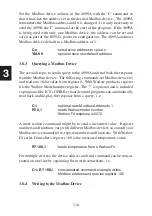
The 4899A generates a service request (SRQ) whenever any of the enabled 

bits in the Status Byte Register become true and the 4899A is not addressed 

as a talker.  The Status Byte Register may be read by a Serial Poll or with 

the 

*STB?

 query.  A Serial Poll resets the RQS bit; the 

*STB?

 query does 

not change the bit.  The Status Byte Register is enabled by setting the 

corresponding bits in the Service Request Enable Register with the 

*SRE


command.  e.g.

*SRE 160


‘Sets the SRE Register to 1010 0000 which  


enables just the Event Status and Questionable   


summary bits to generate SRQs.

3.4.8  Saving the Enable and Transition Register Values

The Enable and Transition Register values can only be saved and recalled 

at power turn-on by disabling the PSC flag.  

The *SAV command does not 

save the Enable and Transition register values.

  Use the *PSC 0 com-

mand to disable the PSC flag and save the current Enable and Transition 

register values.  The following example saves the current settings which 

enables bits in the Operation and Event Status Registers to generate a SRQ 

at power turn-on. e.g.

STAT:OPER:ENAB 1


‘enables bit 1

STAT:OPER:NTR 1


‘enables negative transition

*ESE 192;*SRE 32;*PSC 0


‘saves ESE and SRE bits  


 as power on settings. 

Note that the enable and transition commands must be on the same line or 

set prior to the *PSC 0 command to be saved.  A later *PSC 1 command 

sets the PSC flag which will cause the registers to be cleared at the next 

power turn-on.  The Enable and Transition Register values can be set or 

changes at any time by program commands.

3.4.9  488.2 Differences from 488.1 Devices

The IEEE 488.1 Device Clear command 

does not

 reset the unit’s input-

output settings as would be expected of a 488.1 device.  To reset the unit’s 

input-output settings, use the *RST (Reset) or *RCL 0 command.

3.5 

488.2 CONFORMANCE INFORMATION 

Summary of Contents for 4809A

Page 1: ...ICS ELECTRONICS ICS a division of Systems West Inc MODEL 4809A 4819A 4829A and 4899A GPIB Modbus Interfaces Instruction Manual MODBUS...

Page 2: ...us Interface Instruction Manual 7034 Commerce Circle Pleasanton CA 94588 Phone 925 416 1000 Fax 925 416 0105 Publication Number 120148 Web Site http www icselect com April 2017 Edition Rev 19 ICS ELEC...

Page 3: ...ications The Model 4899A has been tested and found to comply with the limits for a Class A computing device pursuant to Subpart J of Part 15 of the FCC Rules and to comply with the EEC Standards EN 55...

Page 4: ...ion Description GPIB Addressing 488 2 Commands SCPI Commands Modbus Commands Programming Guidelines and OEM Documentation Theory of Operation Block diagram Description Maintenance Troubleshooting and...

Page 5: ...ii This page left intentionally blank...

Page 6: ...4829A 4899A GPIB Modbus Interfaces are IEEE 488 2 GPIB to Serial Interfaces with special firmware to control Modbus RTU Slave devices from the GPIB or HP IB bus They let the user send simple commands...

Page 7: ...second connector mates to one of ICS s GPIB Connector Address SwitchAssemblies which mount a GPIB connector and an GPIB address switch on the rear panel of the host chassis ICS s GPIB Connector Addres...

Page 8: ...ac Adapter B Ship with British 230 Vac Adapter E Ship with European 230 Vac Adapter Base Model Number 4899A Minibox Product 4809A Board Product 114922 4809A board only version 4819A Board Product 1151...

Page 9: ...es Primary addresses 0 30 1 4 3 Buffers GPIB input 2 kbytes GPIB output 1 kbytes Serial input output 256 bytes 1 4 4 488 2 Common Commands The4899AconformstoIEEESTD488 2 19A87 Whenaddressedtolistenin...

Page 10: ...l pairs together for 2 wire networks The RX pair includes a termination network for biasing 2 wire networks Signal pinouts are listed in Table 2 4 1 5 1 Modbus RTU Messages Messages conform to the Mod...

Page 11: ...RS 485 Specifications The 4809A 4829A and 4899A have differential RS 485 line drivers and receivers that provide RS 422 and RS 485 compatible signals The line drivers and receivers are designed to ope...

Page 12: ...n Command Functions Factory Setting ADDRess Sets GPIB bus address 4 EXT Enables External GPIB Address Switch OFF 4809A only BAUD Sets transmit receive baud rate 9600 PARity Sets parity type NONE CHECK...

Page 13: ...current GPIB address by blinking the front panel LEDs for one half second The GPIB address is the sum of the binary bit weights The LED bit weights are RDY TALK LSTN SRQ ERR 16 8 4 2 1 Any errors fou...

Page 14: ...4 kg including adapter Temperature Operating 10 C to 55 C Storage 40 C to 70 C Humidity 0 90 RH without condensation Shock Vibration Normal handling only Construction All metal case Power 9 to 32 Vdc...

Page 15: ...1 10 1 Figure 1 1 4899A Outline Dimensions 18 92 cm Side View 14 15 cm End View 3 86 cm 254 cm 0 95 cm max connector...

Page 16: ...to 55 C Storage 40 C to 70 C Humidity 0 90 RH without condensation Shock Vibration Normal handling only Construction Flame retardant printed circuit board Power 5 0 25 Vdc 300 MA regulated 5 5 to 12 V...

Page 17: ...ULL PWR TLK BSY 1 4819A or 4829A J1 GPIB Connector J2 Serial Connector J3 Device Serial Connector Status LEDs 4 50 4 00 0 190 dia mounting holes 4 plcs 0 300 dia mounting pads Mounting Blocks 2 plcs 0...

Page 18: ...condensation Shock Vibration Normal handling only Construction Flame retardant printed circuit board Connector shells grounded to chassis supports and mounting brackets Power 5 0 25 Vdc 300 MA regula...

Page 19: ...S EMI RFI Meets limits for part 15 Class A of US FCC Docket 20780 and complies with EEC Standards EN 55022 and 50082 1 CE Certificate of Compliance reproduced in Figure 1 4 UL CSA VDE AC Wall adapter...

Page 20: ...rer s Address 473 Los Coches Street Milpitas CA 95035 USA Importer s Name Importer s Address Type of equipment GPIB to Serial Converter Model No 4899 Serial No Thru Year of manufacturer I the undersig...

Page 21: ...4829A 4899A Instruction Manual 113640 L Horizontal GPIB Connector Address Switch Assembly Dash number is cable length from 10 to 90 CM long 90 CM standard 113642 L VerticalGPIBConnector AddressSwitch...

Page 22: ...ll make arrangements for the unit to be repaired or replaced without waiting for the claim against the carrier to be settled 2 2 SHIPMENT VERIFICATION Take a moment to verify the shipment Each shipmen...

Page 23: ...mounting kit 4 Connect the AC adapter to the 4899A and to the AC power Turn the unit on and verify that it passes its selftest and that it indicates the correct GPIB address Use the IDN query to verif...

Page 24: ...to the power supply to avoid noise problems Set jumper W1 to REG for unregulated 5 5 12 volt power to P1 for regulated 5 volt power 5 Plug in the GPIB and serial cables and connect the unit to the GPI...

Page 25: ...rd and mounting blocks 2 Mounting holes are 0 150 dia thru 3 Cutout A is 1 575 in x 0 625 in with 0 150 dia holes 4 Cutout B is 0 875 in x 0 450 in D shell with 10 slope to bottom and with 0 125 dia h...

Page 26: ...tings in Table 1 1 to determine if your unit needs to be reconfigured before it can send data to the serial device If the board needs to be reconfigured follow the instructions in Sections 2 4 2 8 to...

Page 27: ...easiest way to configure the unit is to use ICS s Minibox configuration program niconf_w exe which guides the user through a menu driven configuration procedure niconf_w exe runs withanyICS NationalIn...

Page 28: ...un and display the Support CD Selection Window Click Configure GPIB Interfaces to run the niconf_w exe program or Install Keyboard Utilities to install the GPIBkybd program You can always download nic...

Page 29: ...PIB Bus Cable AC Adapter 4899A PC with GPIB Controller Card a 4899A Configuration Setup Connect the 4809A 4819A or 4829A to the GPIB controller card in the PC or to a USB GPIB Controller as shown in F...

Page 30: ...4 04 10 and click the SET button The factory default set ting is 4 If you do not know the unit s GPIB address turn the unit off and back on The unit will blink its GPIB address on the front panel LED...

Page 31: ...ter Y to set PSC 0 N to set PSC 1 or click the appropriate boxes The program may ask if you want to lock the parameters so that they cannot be changed by the end user The configuration program automat...

Page 32: ...the GPIB controller as shown in Figure 2 2 Run the program and if required use anAbort REN or a take control type command to have the bus controller assert REN Then turn the unit on 2 Determine the un...

Page 33: ...a response if you just press Send The following example shows how to change and query the baud rate SYST COMM SER BAUD 19200 sets the baud rate SYST COMM SER BAUD queries the baud rate should reply 1...

Page 34: ...hat one of the connectors be used to connect it to the GPIB bus The unused connector should be left open 2 8 2 1 GPIB Connector J1 TheGPIBSignal pinassignmentsforJ1areidenticaltoastandardIEEE 488 conn...

Page 35: ...the 4809Areads the five address lines ADSW1 ADSW5 if the external address switch is enabled Connector J2 mates with ICS s GPIB Connector Address Switch Assem blies These assemblies are small business...

Page 36: ...1 1 LSB ADSW3 8 GRY 1 4 ADSW2 9 WHT 1 2 NRFD 10 BLK 1 GPIB Signals REN 11 BRN2 DAV 12 RED 2 IFC 13 ORG 2 NDAC 14 YEL 2 EOI 15 GRN 2 ATN 16 BLU 2 SRQ 17 VIO 2 DIO1 18 GRY 2 DIO2 19 WHT 2 DIO3 20 BLK 2...

Page 37: ...4 to drive remote LEDs Each signal is low true and can sink 3 mA Use a resistor in series with 5 Vdc to limit the current to LED Connect the LED cathodes to the driver signals The recommended resistor...

Page 38: ...Send A Data Set Ready Ground Signal Detected A Signal Detected B Clear to send B Send Data B Receive Data B 4809A Talk LED Dvr Request to send B Data Terminal Rdy A 4809A Listen LED Dvr Data Terminal...

Page 39: ...ce The RxD and TxD pins can be exchanged by rotating jumpers W4 90 degrees DCD and DSR are pulled up to an ON state and RTS is jumpered back to CTS 2 9 3 4829A Serial Connections The 4829A has two rig...

Page 40: ...torwithSDandRDdifferentialsignal pairs The SD and RD signal pairs are a four wire full duplex interface The SD and RD signal pairs can be jumpered together on the 4829A board for half duplex operation...

Page 41: ...A RS 232 connection to a Watlow F4 Temperature Controller Both interfaces transmit on pin 2 and receive on pin 3 1 2 3 4 5 6 7 25 4899A or 4809A WATLOW F4 4899A 4809A TXD RXD 1 12 13 14 15 16 Figure 2...

Page 42: ...work so the Modbus can respond to the message Two wire RS 485 networks also need termination networks to bias the lines inthe mark statewhenneitherunitistransmitting Theterminationnetworks are made up...

Page 43: ...c and ground provided by the Watlow F4 Temperature Controllers 1 2 14 3 16 7 25 4899A or 4809A WATLOW F4 1 11 12 13 14 15 16 WATLOW F4 T R T R 1K 1K 120 1 11 12 13 14 15 16 Figure 2 14 RS 485 Network...

Page 44: ...RS 485 Network connections to a Watlow EZ Zone Controller Figure 16 shows an 4829A driving a single Watlow EZ Zone Controller with it RS 485 output The 4829A has an internal termination network with...

Page 45: ...REG P1 for direct regulated 5 Vdc power REG for unregulated DC power W2 Set for EPROM size Not user changeable 512 W3 Write Enable Installed enables saving setup parameters Installed in EEPROM Remove...

Page 46: ...5 Vdc regulated power source REG selects the regulator output for 5 5 to 15 Vdc power W3 Default Install and power cycle the unit to reset the unit to Omitted its factory default settings Leave out fo...

Page 47: ...ut for 5 5 to 15 Vdc power W3 Default Install and power cycle the unit to reset the unit to Omitted its factory default settings Leave out for normal operation W4 Connects SD pair to RD signal pair In...

Page 48: ...its case fitting the PC board into the tracks on each side of the case Be sure the switch and LEDs are correctly aligned before pushing the switch through the front panel Replace the two rear panel s...

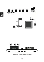
Page 49: ...2 28 2 UP W8 W3 WR ENA W9 W6 Serial GPIB SW Y1 U14 W1 422 232 CT CV CT CV W7 W5 W4 422 232 422 232 CT CV PRL DEFAULT Figure 2 20 4899A Jumper Locations...

Page 50: ...n the rack mounting kit Push the unit down until it rests flat on the kit and the feet are in the four holes 2 Repeat step 1 for a second unit if two units are being held in one rack mounting kit 3 Al...

Page 51: ...2 30 2 This page left intentionally blank...

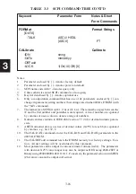
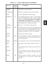
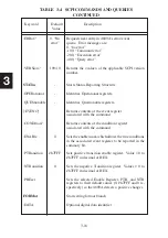
Page 52: ...he 4899A responds to three types of commands 1 IEEE 488 2 Common Commands in Table 3 2 These include the IDN and ESR queries and the SAV 0 save command 2 SCPI Commands in Table 3 3 are for setting int...

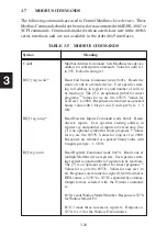
Page 53: ...o the 4899Aover the GPIB bus the 4899Acommunicates with the selected Modbus device Modbus commands should not be mixed or concatenated with IEEE 488 2 or SCPI commands If the 4899A s message packet is...

Page 54: ...er can control an RS 232 Modbus device from the serial connector or from the 4819A s GPIB interface However both interfaces cannot be used at the same time Once the GPIB interface is activated the ser...

Page 55: ...for address setting instructions 3 3 2 4809AAddress External Address Switch The 4809A s GPIB address can also be set by connecting the 4809A to an external address switch Connector J2 contains the ext...

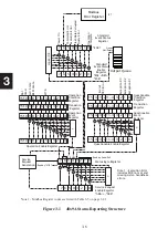
Page 56: ...d or that the 4899A needs service There are four major sources of SRQs each of which is summarized in a bit in the Status Byte Register Three of the sources are event registers with their own enabling...

Page 57: ...3 6 3 Flash Data Corrupted Figure 3 1 48x9A Status Reporting Structure Note 1 Modbus Register codes are listed in Table 3 5 on page 3 22...

Page 58: ...mplete event has no meaning for either unit Table 3 1 ESR BIT DEFINITIONS Bit Bit Event Description Weight 7 128 PON The Power on event occurs at power turn on and can be used to signal a power off on...

Page 59: ...to the Question able Event Register The Questionable Event Register bits becomes true 1 when the positive transition bit is enabled and the associated condition register bit makes a 0 to 1 transition...

Page 60: ...orts the WTG Waiting for Trigger status and the Local Lockout and Remote GPIB interface states The WTG bit is true when the 4899A has been armed and is waiting for a trigger The following commands dem...

Page 61: ...values Use the PSC 0 com mand to disable the PSC flag and save the current Enable and Transition register values The following example saves the current settings which enables bits in the Operation a...

Page 62: ...y if CLS is the first message in the com mand line Sets Event Status Enable Register to value value is an integer between 0 and 255 whose binary equivalent cor responds to the state 1 or 0 of bits in...

Page 63: ...ted 4899A operations have been finished Places an ASCII character 1 into the 4899A s Output Queue when all pend ing selected 4899A operations have been finished Controls the automatic power on clearin...

Page 64: ...e is an integer be tween 0 and 255 whose binary equivalent corresponds to the state 1 or 0 of bits in the register If value is not between 0 and 255 an Execution Error is generated 4899A returns the v...

Page 65: ...noted The SCPI commands are not case sensitive The portion of the command shown in capitals denotes the abbreviated form of the keyword Either the abbreviated or whole keyword may be used when enteri...

Page 66: ...RS485 0 1 or OFF ON 0 ERRor 0 No error VERSion 1994 0 STATus OPERation Status Inputs WTG EVENt bit 0 1 and 5 active 0 CONDition bit 0 1 and 5 active 0 ENABle bit 0 1 and 5 active 0 ENABLE PTRansition...

Page 67: ...re required A list of numbers is separated by commas or uses a colon to denote a range of numbers 8 Numeric entries conform to IEEE 488 2 section 7 7 2 4 for decimal numeric param eters 9 ASCII format...

Page 68: ...nenablesthe4809A sexternaladdressswitchinputsto be used to input a switch setting for the GPIB address Off uses the value saved in E2 ROM memory Does not apply to the 4899A Values 0 1 or OFF ON SERial...

Page 69: ...condition register associated with the command ENABle 0 Sets the enable mask which allows the true conditions in the associated event register to be reported in the summary bit PTRansition h7FFF Sets...

Page 70: ...function CALibrate Starts calibrate branch IDN string Sets user IDN message String is up to 72 characters and consists of four fields manufacturer model code serial number and firmware revision separ...

Page 71: ...s a packed binary value with 1 bit per coil 8 coils per byte 1 ON RI reg ninp Read Discrete Inputs Command code 0x02 Reads discrete inputs User specifies starting address in register reg and number of...

Page 72: ...oating point value in low byte to high byte order The specified register reg contains the lower two bytes and the next higher register contains the upper two bytes WC reg b Write Coil Command code 0x0...

Page 73: ...imeout setting E Read Error Command Reads and clears the Modbus Error Register and bit 6 in the Event Status Register Returns a error code whose value is 0 to 255 Current error values are 0 No errors...

Page 74: ...rors and confusing the GPIB to Modbus Interface 3 8 1 General Configuration Guidelines New units are factory set so that they are ready to be used when received Table 1 1 lists the Factory Configurati...

Page 75: ...ead one 16 bit value from register 0 With Watlow products register 0 is the Watlow Model number register The is optional and is included so programs like ICS s GPIB Keyboard control programs can autom...

Page 76: ...6 bit registers The value is assumed to have three decimal places 3 8 6 32 Bit Write To write a set point of 1250 degrees which is really 1250 000 to Regis ters 27 and 28 multiply the setpoint value S...

Page 77: ...laces Reading MSW 65536 LSW 1000 3 8 8 Floating Point Variables Some new Modbus devices like Watlow s EZ PM series controllers use two consecutive register to control a value or to read back a process...

Page 78: ...e cific Modbus device Some devices fail to respond within the default time period because they perform periodic calibrations The recommendation is that your program should have a built in recovery rou...

Page 79: ...ause and clear the SRQ so another error will cause another SRQ In case one this is done by reading the Modbus Error Register with the E query In case two the Questionable Event Register must be read t...

Page 80: ...ngs The saved configuration is recalled and the I O settings restored to their saved state at power turn on or by the RCL 0 command WARNING Because the Nonvolatile Memory has a finite number of write...

Page 81: ...ture The OEM needs to define what the digital inputs mean if they are part of the system how to enable SRQs and how to read the registers The SCPI Standard requires that the SCPI command tree and SCPI...

Page 82: ...IEEE 488 bus and a Modbus slave device over a serial link The 4899A is made up of seven major elements most of which are interconnected to the microprocessor by a common data address and control sign...

Page 83: ...utted at the serial interface SCPI commands and IEEE 488 2 commands are parsed and used to set control parameters perform an operation or query a parameter Responses are placed in the GPIB buffer so t...

Page 84: ...ys its current GPIB address setting on the front panel LEDs Bit weights are read from right to left with the least significant bit on the far right The RDY LED comes on to indicate a successful comple...

Page 85: ...PI commands and IEEE 488 2 commands are parsed and used to set the 4819A s configura tion perform an operation or query a parameter Responses are placed in the GPIB buffer so they can be returned to t...

Page 86: ...he front panel The error pattern is repeated until the unit is turned off Just after completing the self test routine the 4819A displaysitscurrentGPIBaddresssettingonitsLEDs TheRDYLEDcomes on to indic...

Page 87: ...to 12 volt DC power to 5 Vdc to run the 4819A s circuits A jumper on the 4819A bypasses the regulator so that the 4819A can be run from regulated 5 volt DC power A DC DC converter in the RS 232 transm...

Page 88: ...coming serial mes sage is buffered and then retransmitted to the internal serial device The serial signals to the internal device are differential RS 485 signals Internal jumpers connect the transmit...

Page 89: ...4 8 4 This page intentionally left blank...

Page 90: ...ver if the interfaces are used in an application where the IEEE 488 bus cables are frequently changed or if the input signals appear erratic the GPIB connector may require clean ing to remove wax and...

Page 91: ...listed in Table 5 1 5 3 2 Operating Failures Use the fault isolation information in Table 5 2 to narrow the operational problem down to a specific area The majority of installation faults can be fixed...

Page 92: ...899A U7 in 4809A or U2 in 4819A Defective Flash that cannot be written to Replace part DefectivedecoderGAL Testand orreplace GAL U3 in 4899A U16 in 4809A or U5 in 4819A Flash loose in its socket or ha...

Page 93: ...ress setting Wrong firmware or GPIB chip for hardware configuration Check hardware configuration andchangefirmwareorreplaceGPIB Control ler chip with NI 7210 U8 in 4819A Wrong CPU type Should be Zilog...

Page 94: ...Unit shows a blinking Self test fault Check Self Test errors in LED at power turn on Table 5 1 ERR LED on at Flash data lost Use CLS to clear the LED power turn on Use CAL DATE command to enternewdate...

Page 95: ...th the E command No communication Wiring error CheckRS 232orRS 485 with Modbus device cablewiringagainstfigures in Section 2 Modbus TXD signal must go to 48x9A receive input Use an RS 232TrackerorDVMt...

Page 96: ...s CheckModbusErrorregister for Modbus problems Faulty or missing Modbus timeout Check Modbus Error Register Modbus responses setting withtheE queryforatime out error Error 101 UseDcommandtolengthen ti...

Page 97: ...ettings If that does not work use the hardware default jumper 1 Power the board off 2 Locate the default jumper and place a shorting jumper on it See Section 2 11 for jumper locations 3 Power the boar...

Page 98: ...ved over the phone as opposed to returning a unit for repair 2 Write a description of the problem and attach it to the material be ing returned Describe the installation system failure symptoms and ho...

Page 99: ...5 10 5 This page left intentionally blank...

Page 100: ...ial Data Communications Background A 15 A2 1 Introduction to Serial Communication A 15 A2 2 RS 232 Standard A 18 A2 3 RS 422 and RS 485 Standards A 20 A2 4 RS 530 Pinouts A 21 A2 5 Serial Interface Pr...

Page 101: ...controller protocols are built in to the PC2 drivers All IEEE 488 2 common commands queries and SCPI com mands are placed in the output command string by the user and are not part of the PC2 driver so...

Page 102: ...lersandmanydevices theIEEE488driverspecifications limit the total number of units on one bus system to 15 Only one controller can be the controller in charge at any given time Control originates with...

Page 103: ...s set true by the control ler in charge while it is sending interface messages or device addresses The messages are transmitted on the seven least significant data lines and are listed in the MSG colu...

Page 104: ...mmands MLA My listen address controller to self MTA My talk address controller to self LAD Device listen address TAD Device talk address SAD Secondary Device address device optional ad dress UNL Unlis...

Page 105: ...D GROUP LISTEN ADDRESS GROUP TALK ADDRESS GROUP SECONDARY COMMAND GROUP PRIMARY COMMAND GROUP PCG LSD MSD MSG GTL SDC PPC GET TCT ASCII DLE DC1 DC2 DC3 DC4 NAK SYN ETB CAN EM SUB ESC FS GS RS US MSG L...

Page 106: ...7 8 9 10 11 12 13 14 15 16 17 18 19 20 21 22 23 24 DIO5 DIO6 DIO7 DIO8 REN GND TW PAIR W DAV GND TW PAIR W NRFD GND TW PAIR W NDAC GND TW PAIR W FC GND TW PAIR W SRQ GND TW PAIR W ATN SIGNAL GROUND D...

Page 107: ...ntrol Operation Complete Standard Event Status Register ESR 7 6 5 4 3 2 1 0 7 6 5 4 3 2 1 0 Logical OR Standard Event Status Enable Register ESE NRf ESE Queue Not Empty 7 5 4 3 2 1 0 Logical OR 7 6 3...

Page 108: ...expected A1 2 2 IEEE 488 2 Reporting Structure With IEEE 488 2 status reporting was enhanced from the simple serial poll response byte in IEEE 488 1 to the multiple register concept shown in Figure A...

Page 109: ...Command Devices that support parallel polls must support the following three com mands IST Individual Status Query PRE Parallel Poll Register Enable Command PRE Parallel Poll Register Enable Query De...

Page 110: ...tatus Byte Register contents plus the MSS bit in response to a STB query The MSS bit is cleared when the condi tion is cleared 488 2 restricts the Device Clear to only clearing the device s buffers an...

Page 111: ...age and syntax Asecond benefit of SCPI is that its English like structure and words are self documenting eliminatingtheneedsforcommentsexplainingcrypticinstru ment commands A third benefit is the redu...

Page 112: ...uts it back at the root node IEEE 488 2 common commands and queries can be freely mixed with SCPI messages in the same programmessagewithoutaffectingtheaboverules FigureA 5showssome compound command e...

Page 113: ...re used as a way of listing multiple values Channel lists are enclosed in parenthesis and start with the ASCII character The values are separated with commas The length of the channel list is determin...

Page 114: ...rmat Typical computer baud rates and their uses are 110 for old mechanical teletypes 300 1200 for low speed devices an older modems 9600 to 38400 baud for high speed devices and newer modems Data form...

Page 115: ...form as single 8 bit characters or in hex form as a pair of the ASCII characters 0 through 9 and A through F Each Hex character represents 4 binary bits so two Hex characters are needed for each 8 bit...

Page 116: ...to convert the serial data bits into tones that will pass through the telephone system s 300 to 3000 Hz voice band For low baud rates up to 1200 Hz the modems convert the bits into two tones frequenc...

Page 117: ...opping any line normally means the receiving device s buffer is full or it is busy with the last message Another method of controlling the data flow is to imbed X on X off char acters in the data mess...

Page 118: ...lly RS 232 signals are bipolar and are referenced to a common ground AB on pin 7 Transmitted signals must be between 5 and 15V or 5 and 15V into 3000 to 7000 ohm loads Maximum open circuit transmit te...

Page 119: ...ngle ended RS 232signals TheRS 422differentialsignalsrequireadifferentialreceiver and are not referenced to Signal Ground Differential transmitted signals applied to the interconnecting cable are 2 to...

Page 120: ...nals A2 5 Serial Interface Problems Most of the problems that arise when connecting serial devices can be avoided if the user will compare the signals on both devices interfaces before plugging them t...

Page 121: ...r as shown in Figure A 9 b The Address Switch is an eight position rocker switch For ICS board products the five left most switches set the GPIB address The bit weights are shown in Figure A 10 Up is...

Page 122: ...a on the host chassis rear panel as shown in Figure A 11 Leave enough room inside for the flat ribbon cable bend radius 3 Machine the cutouts shown in Figure A 12 If the rear panel is thicker than 0 0...

Page 123: ...e to the board so it avoids any high RFI or electrical noise area Plug the cable into J2 6 Mark or silkscreen the switch functions onto the rear panel as shown in Figure A 10 Identify the 5 address ro...

Page 124: ...3 Holes are 0 180 dia 2 plcs 4 Allow 0 25 inches for cable bend radius 0 920 0 420 1 578 1 842 1 200 0 635 Notes 1 All dimensions are in inches 2 D cutout radius is 0 2 inches 3 Holes are 0 180 dia 2...

Page 125: ...A 26 A3 This page intentionally left blank...

Page 126: ...Specifications 1 13 Serial Connections 2 16 Watlow 96 Connections 2 21 4829A Block Diagram 4 6 Block Diagram Description 4 6 Description 1 2 EZ Zone connections 2 23 Installation Guide 2 4 Jumper sett...

Page 127: ...1 Connections GPIB 2 13 Serial 2 16 Connector Switch Board Assembly A 23 Cable length A 22 Cutouts A 25 Connectors 4809 1 11 4819 1 13 4899 1 9 Copyright release 3 30 D Digital Inputs Monitoring chang...

Page 128: ...4 488 2 Conformance information 3 11 488 2 required status reporting capabilities A 7 A 8 488 2 status reporting structure 3 5 Address ranges 1 4 Bus Figure A 3 SCPI commands A 12 SCPI command structu...

Page 129: ...3 2 5 1 Theory of 4 1 Operational Registers 3 9 Outline dimensions 4819 1 12 Output Queue 3 10 P Physical 4809 1 11 4819 1 13 4899 1 9 Programmable functions 1 7 Programming 32 bit variables 3 25 3 2...

Page 130: ...1 5 Serial Interface Baud rates 1 5 Data character formats 1 6 Problems A 21 Shipment Verification 2 1 Specifications 1 3 RS 232 1 6 RS 485 RS 422 1 6 SRQs Generating from Modbus Errors 3 28 Standard...

Page 131: ...I Index 6 This page left intentionally blank...

Reviews: