10. Endian Mapping
182
PowerSpan II User Manual
80A1010_MA001_09
Integrated Device Technology
www.idt.com
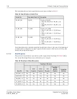
The byte lane to register address mapping is shown in
. Only munged cases are illustrated. The
PB slave asserts PB_TEA_ in response to an unaligned access to a register if the END bit is set for
PowerPC little-endian mode.
A PCI transaction is generated by accessing the following registers:
•
Processor Bus Configuration Cycle Data register (PB_CONF_DATA)
•
Processor Bus to PCI-1 Interrupt Acknowledge Cycle Generation register (PB_P1_IACK)
•
Processor Bus to PCI-2 Interrupt Acknowledge Cycle Generation register (PB_P2_IACK)
The endian conversion scheme applied for processor bus access to these registers is controlled by the
END bit, but the endian mapping scheme in this case is described in
Table 50: PowerSpan II PowerPC Little-Endian PB Register Accesses
Transfer
Size
Starting
Address
(Munged)
PB_A
[29:31]
PowerPC Byte Lanes
PowerSpan II Register Address
A[2]
A[1:0]
0
1
2
3
4
5
6
7
11
10
01
00
Byte
000
D0
1
D0
001
D1
1
D1
010
D2
1
D2
011
D3
1
D3
100
D4
0
D4
101
D5
0
D5
110
D6
0
D6
111
D7
0
D7
Two bytes
000
D0
D1
1
D0
D1
010
D2
D3
1
D2
D3
100
D4
D5
0
D4
D5
110
D6
D7
0
D6
D7
Word
000
D0
D1
D2
D3
1
D0
D1
D2
D3
100
D4
D5
D6
D7
0
D4
D5
D6
D7

