Document Number: 002-14826 Rev. *G
Page 34 of 65
PRELIMINARY
CYW43903
10. GPIO Signals and Strapping Options
10.1 Overview
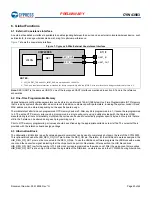
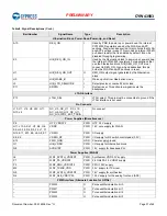
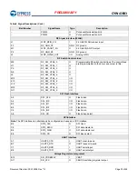
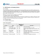
This section describes GPIO signals and strapping options. The pins are sampled at power-on reset (POR) to determine various
operating modes. Sampling occurs a few milliseconds after an internal POR or deassertion of the external POR. After the POR, each
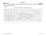
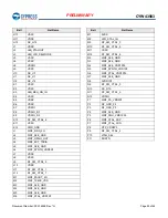
pin assumes the GPIO or alternative function specified in
. Each strapping option pin has an internal pull-up (PU) or pull-down
(PD) resistor that determines the default mode. To change the mode, connect an external PU resistor to VDDIO or a PD resistor to
ground, using a 10 kΩ resistor or less.
Note:
Refer to the reference board schematics for more information.
10.2 Weak Pull-Down and Pull-Up Resistances
At VDDO = 3.3V ±10%, the minimum, typical, and maximum weak pull-down resistances (for a pin voltage of VDDO) are 37.99 kΩ,
44.57 kΩ, and 51.56 kΩ, respectively. At VDDO = 3.3V ±10%, the minimum, typical, and maximum weak pull-up resistances (for a
pin voltage of 0V) are 34.73 kΩ, 39.58 kΩ, and 44.51 kΩ, respectively.
10.3 Strapping Options
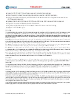
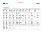
provides the strapping options.
Table 9. Strapping Options
Pin Name
Strap
#
Default Internal
Pull During
Strap
Description
GPIO_1
GSPI_MODE
D1
PD
Enable gSPI interface
GPIO_7
WCPU_BOOT_MODE
E5
PD
Boot from SoC SROM or SoC SRAM
GPIO_11
ACPU_BOOT_MODE
B1
PD
Boot from tightly coupled memory (TCM) ROM or TCM
RAM
GPIO_13
SDIO_MODE
E8
PD
Select either SDIO host mode or SDIO device mode
GPIO_15
VTRIM_EN
A2
PD
Enable PMU voltage trimming
RF_SW_CTRL_5
DAP_CLK_SEL
M10
PD
Select XTAL clock or the test clock (tck) for the debug
access port (DAP)
RF_SW_CTRL_7
RSRC_INIT_MODE
L12
PD
PMU resource initialization mode selection

