2004 Microchip Technology Inc.
Advance Information
DS70119B-page 23
dsPIC30F6010
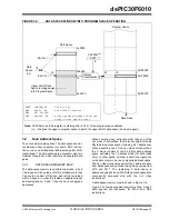
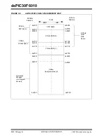
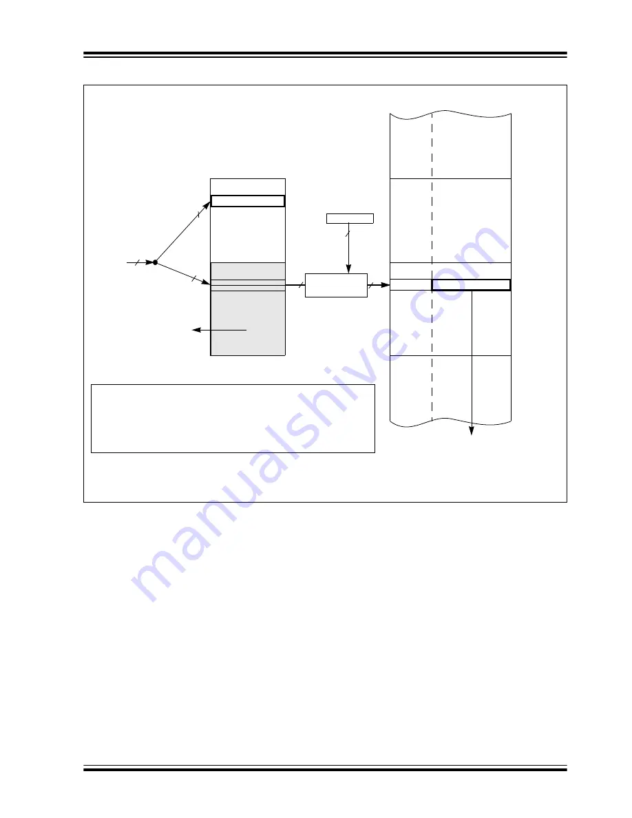
FIGURE 3-5:
DATA SPACE WINDOW INTO PROGRAM SPACE OPERATION
3.2
Data Address Space
The core has two data spaces. The data spaces can be
considered either separate (for some DSP instruc-
tions), or as one unified linear address range (for MCU
instructions). The data spaces are accessed using two
Address Generation Units (AGUs) and separate data
paths.
3.2.1
DATA SPACE MEMORY MAP
The data space memory is split into two blocks, X and
Y data space. A key element of this architecture is that
Y space is a subset of X space, and is fully contained
within X space. In order to provide an apparent linear
addressing space, X and Y spaces have contiguous
addresses.
When executing any instruction other than one of the
MAC
class of instructions, the X block consists of the 64
Kbyte data address space (including all Y addresses).
When executing one of the
MAC
class of instructions,
the X block consists of the 64 Kbyte data address
space excluding the Y address block (for data reads
only). In other words, all other instructions regard the
entire data memory as one composite address space.
The
MAC
class instructions extract the Y address space
from data space and address it using EAs sourced from
W10 and W11. The remaining X data space is
addressed using W8 and W9. Both address spaces are
concurrently accessed only with the
MAC
class
instructions.
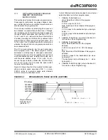
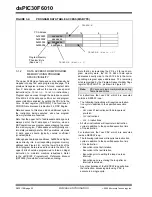
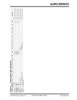
A data space memory map is shown in Figure 3-6.
Figure 3-7 shows a graphical summary of how X and Y
data spaces are accessed for MCU and DSP
instructions.
23
15
0
PSVPAG
(1)
15
15
EA<15> =
0
EA<15> =
1
16
Data
Space
EA
Data Space
Program Space
8
15
23
0x0000
0x8000
0xFFFF
0x21
0x108000
0x10FFFF
Data Read
Upper half of Data
Space is mapped
into Program Space
Note:
PSVPAG is an 8-bit register, containing bits <22:15> of the program space address
(i.e., it defines the page in program space to which the upper half of data space is being mapped).
0x108200
Address
Concatenation
BSET
CORCON,#2
; PSV bit set
MOV
#0x21, W0
; Set PSVPAG register
MOV
W0, PSVPAG
MOV
0x8200, W0
; Access program memory location
; using a data space access
Summary of Contents for dsPIC30F6010
Page 12: ...dsPIC30F6010 DS70119B page 10 Advance Information 2004 Microchip Technology Inc NOTES...
Page 32: ...dsPIC30F6010 DS70119B page 30 Advance Information 2004 Microchip Technology Inc NOTES...
Page 38: ...dsPIC30F6010 DS70119B page 36 Advance Information 2004 Microchip Technology Inc NOTES...
Page 50: ...dsPIC30F6010 DS70119B page 48 Advance Information 2004 Microchip Technology Inc NOTES...
Page 68: ...dsPIC30F6010 DS70119B page 66 Advance Information 2004 Microchip Technology Inc NOTES...
Page 72: ...dsPIC30F6010 DS70119B page 70 Advance Information 2004 Microchip Technology Inc NOTES...
Page 76: ...dsPIC30F6010 DS70119B page 74 Advance Information 2004 Microchip Technology Inc NOTES...
Page 86: ...dsPIC30F6010 DS70119B page 84 Advance Information 2004 Microchip Technology Inc NOTES...
Page 108: ...dsPIC30F6010 DS70119B page 106 Advance Information 2004 Microchip Technology Inc NOTES...
Page 116: ...dsPIC30F6010 DS70119B page 114 Advance Information 2004 Microchip Technology Inc NOTES...
Page 128: ...dsPIC30F6010 DS70119B page 126 Advance Information 2004 Microchip Technology Inc NOTES...
Page 150: ...dsPIC30F6010 DS70119B page 148 Advance Information 2004 Microchip Technology Inc NOTES...
Page 164: ...dsPIC30F6010 DS70119B page 162 Advance Information 2004 Microchip Technology Inc NOTES...
Page 208: ...dsPIC30F6010 DS70119B page 206 Advance Information 2004 Microchip Technology Inc NOTES...
Page 220: ...dsPIC30F6010 DS70119B page 220 Advance Information 2004 Microchip Technology Inc NOTES...
Page 221: ...2004 Microchip Technology Inc Advance Information DS70119B page 221 dsPIC30F6010 NOTES...

