MDDR Subsystem
Microsemi Proprietary UG0446 User Guide Revision 7.0
102
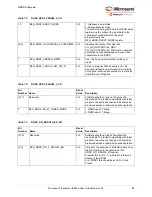
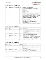
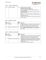
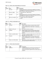
[15:0]
DDRC_LCB_MASK
0×0
64 bits are split into four registers.
[63:48] bits of DDRC_LCB_MASK.
Indicates the mask of the corrected data.
1: On any bit indicates that the bit has been corrected by the
DRAM SECDED logic.
0: On any bit indicates that the bit has NOT been corrected by the
DRAM SECDED logic.
Valid when any bit of DDRC_REG_ECC_CORRECTED_ERR is
High.
This mask does not indicate any correction that has been made in
the SECDED check bits.
If there are errors in multiple lanes, this signal will have the mask
for the lowest lane.
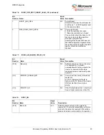
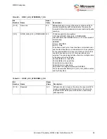
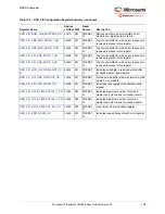
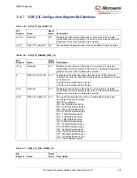
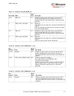
Table 100 •
DDRC_ECC_INT_SR
Bit
Number Name
Reset
Value
Description
[31:3]
Reserved
0×0
Software should not rely on the value of a reserved bit. To provide
compatibility with future products, the value of a reserved bit
should be preserved across a read-modify-write operation.
[2:0]
DDRC_ECC_STATUS_SR
0×0
Bit 0: 1 Indicates the SECDED interrupt is due to a single error.
Bit 1: 1 Indicates the SECDED interrupt is due to a double error.
Bit 2: Always 1
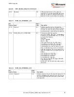
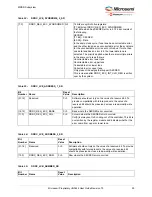
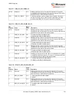
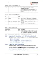
Table 101 •
DDRC_ECC_INT_CLR_REG
Bit
Number Name
Reset
Value
Description
[31:1]
Reserved
0×0
Software should not rely on the value of a reserved bit. To provide
compatibility with future products, the value of a reserved bit
should be preserved across a read-modify-write operation.
0
DDRC_ECC_INT_CLR_REG 0×0
This register should be written by the processor when it has read
the SECDED error status information. This helps to clear all the
SECDED status information, such as error counters and other
SECDED registers.
The read value of this register is always 0.
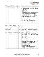
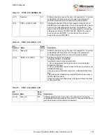
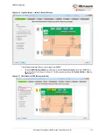
Table 99 •
DDRC_LCB_MASK_4_SR

