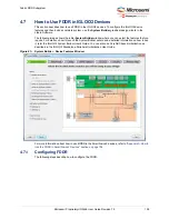
Fabric DDR Subsystem
Microsemi ProprietaryUG0446 User Guide Revision 7.0
154
4.6.9.1
Dynamic DRAM Rank Constraints
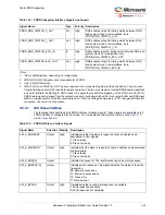
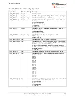
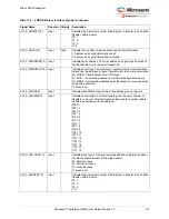
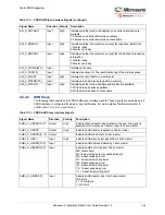
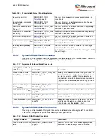
The timing constraints which affect the transactions to a rank are listed in the following table. The control
bit field must be configured as per the DDR memory vendor specification.
4.6.9.2
Dynamic DRAM Global Constraints
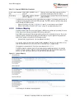
The timing constraints which affect global transactions are listed in the following table. The control bit
field must be configured as per the DDR memory vendor specification.
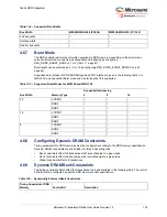
Row cycle time (t
RC
)
REG_DDRC_T_RC,
Minimum time between two successive activates to a
given bank.
Row precharge command
period (t
RP
)
REG_DDRC_T_RP,
Minimum time from a precharge command to the next
command affecting that bank.
Minimum bank active time
(t
RAS(min)
)
REG_DDRC_T_RAS_MIN,
Minimum time from an activate command to a precharge
command to the same bank.
Maximum bank active time
(t
RAS(max)
)
REG_DDRC_T_RAS_MAX,
Maximum time from an activate command to a precharge
command to the same bank.
RAS-to-CAS delay (t
RCD
)
REG_DDRC_T_RCD,
Minimum time from an activate command to a Read or
Write command to the same bank.
Write command period (t
WR
) REG_DDRC_WR2PRE,
Minimum time from a Write command to a precharge
command to the same bank.
Read-to-precharge delay
(t
RTP
)
REG_DDRC_RD2PRE,
Minimum time from a Read command to a precharge
command to the same bank.
Set this to the current value of additive latency plus half of
the burst length.
Table 137 •
Dynamically Enforced Bank Constraints
Timing Constraints of
DDR Memory
Control Bit
Description
Nominal refresh cycle
time (t
RFC(nom)
or t
REFI
)
REG_DDRC_T_RFC_NOM_X32,
Average time between refreshes for a given rank. The
actual time between any two refresh commands may
be larger or smaller than this; this represents the
maximum time allowed between refresh commands
to a given rank when averaged over a large period of
time.
Minimum refresh cycle
time t
RFC(min)
REG_DDRC_T_RFC_MIN,
Minimum time from refresh to refresh or activate.
RAS-to-RAS delay (t
RRD
) REG_DDRC_T_RRD,
Minimum time between activates from bank A to bank
B.
RAS-to-CAS delay (t
CCD
) REG_DDRC_T_CCD,
Minimum time between two reads or two writes (from
bank A to bank B).
Four active window (t
FAW
Sliding time window in which a maximum of 4 bank
activates are allowed in an 8-bank design. In a
4-bank design, set this register to 0x1.
Table 138 •
Dynamic DRAM Global Constraints
Timing Constraint
Control Bit
Description
Read-to-write turnaround
time
REG_DDRC_RD2WR,
Minimum time to allow between issuing any Read
command and issuing any WRITE command
Table 136 •
Dynamically Enforced Bank Constraints

