MDDR Subsystem
Microsemi Proprietary UG0446 User Guide Revision 7.0
6
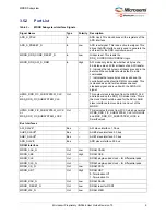
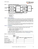
Figure 1 •
System Level MDDR Block Diagram
The MDDR subsystem accepts data transfer requests from AXI or AHB interfaces. Any read/write
transactions to the DDR memories can occur from the following four paths:
•
High performance DMA (HPDMA) controller can access DDR memories through the MSS/HPMS
DDR bridge for high speed data transactions.
•
Other MSS/HPMS masters (for example, FIC_0, FIC_1, and PDMA) can access DDR memories
through the MSS/HPMS DDR bridge.
•
AXI or AHBL masters in the FPGA fabric can access DDR memories through DDR_FIC interface.
Note:
The Cortex-M3 processor can access DDR memories through the MSS DDR bridge for data and code
execution in SmartFusion2.
Note:
The maximum DDR3 data rate supported by MDDR is 333MHz/667Mbps. Therefore, Write Leveling is
not mandatory and the interface works if the board layout includes length matching and follows
SmartFusion2 and IGLOO2 Board Design Guidelines Application Note
. For Read Leveling, Libero SOC
auto-generates pre-defined static delay ratios for MDDR initialization. These delay values are sufficient if
the board layout follows the SmartFusion2/IGLOO2 board-level guidelines.
3.2
Memory Configurations
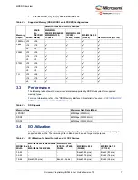
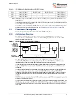
The SmartFusion2 and IGLOO2 FPGA MDDR subsystem supports a wide range of common memory
types, configurations, and densities, as shown in the following table. If SECDED mode is enabled in the
MDDR controller, the external memory module must be connected to the following:
•
Data lines MDDR_DQ_ECC[3:0] when data width is x32
•
Data lines MDDR_DQ_ECC[1:0] when data width is x16
Cache
Controller
S
D
IC
Cortex-M3
Microcontroller
S
D
I
IDC
DS
FIC_0
FIC_1
AHB Bus Matrix
DDR
I/O
FPGA Fabric
AXI/AHB
Master
MSS/HPMS
DDR
Bridge
SmartFusion2/IGLOO2
Blocks in SmartFusion2
DDR
Controller
DDR
PHY
APB Config.
Register
MDDR
AXI
Transaction
Controller
DDR_FIC
64-Bit AXI
HPDMA
MSS/HPMS
DDR
SDRAM
APB
Master
64-Bit AXI /
Single 32-Bit AHBL /
Dual 32-Bit AHBL
16-Bit APB
APB_2


