MDDR Subsystem
Microsemi Proprietary UG0446 User Guide Revision 7.0
29
3.5.5.6.1
Example
In this example, the Address map registers are configured to access a 512 MB DDR3 SDRAM memory
(MT41J512M8RA) from the MDDR subsystem as shown in
"Example 2: Connecting 32-Bit DDR3 to
MDDR_PADs with SECDED" section on page 59
. The 512M x 8-bit DDR3 memory module has
3 bank address lines, 16 rows, and 10 columns.
•
The column address bits 3 to 9 are mapped for system address bit[5] to system address bit[11]. To
map the column 3-bit (C3) to address [5], the field is configured to 3, as the base value is 2. Similarly,
the other column address bits are configured:
•
DDRC_ADDR_MAP_COL_1_CR = 0x3333
•
DDRC_ADDR_MAP_COL_2_CR = 0x3FFF
•
DDRC_ADDR_MAP_COL_3_CR = 0x3300
•
The bank address bits 0 to 2 are mapped for system address bit[12] to system address bit[14]. To
map the bank bit0 to address [12], the field is configured to A, as the base value is 2. Similarly, the
other bank address bits are configured:
•
DDRC_ADDR_MAP_BANK_CR = 0xAAA
•
The row address bits 0 to 15 are mapped for system address bit[15] to system address bit[27]. To
map the bank bit0 to address [15], the field is configured to 9, as the base value is 6. Similarly, the
other bank address bits are configured:
•
DDRC_ADDR_MAP_ROW_1_CR = 0x9999
•
DDRC_ADDR_MAP_ROW_2_CR = 0x9FF
Note:
The MDDR can access the 4 GB address space (0x00000000 - 0xFFFFFFFF). But in this example, 512
MB (0x00000000 - 0x1FFFFFFF) DDR3 SDRAM is connected to the 16 address lines of MDDR. The
memory visible in the other memory space is mirrored of this 512 MB memory.
3.5.5.7
DDR Mode Registers
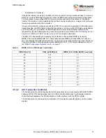
After reset, the DDR controller initializes the mode registers of DDR memory with the values in the
following registers. The mode registers must be configured according to the specification of the external
DDR memory when the controller is in soft reset.
•
•
•
•
The T_MOD and T_MRD bits in
must be configured to the
required delay values. T_MOD and T_MRD are delays between loading the mode registers.
3.5.5.8
SECDED
To enable SECDED mode, set the
bits to 101 in
. The
register must be configured to enable data slice 4 of the PHY.
The register value REG_DDRC_LPR_NUM_ENTRIES in the performance register,
, must be increased by 1 to the value used in Normal mode (without
SECDED).
Note:
MDDR has 36 DQ lines. These data lines are split into the following data slices:
•
Data slice0 represents first 8 DQ lines (DQ0 to DQ7)
•
Data slice1 represents next 8 DQ lines (DQ8 to DQ15)
•
Data slice2 represents next 8 DQ lines (DQ16 to DQ23)
•
Data slice3 represents next 8 DQ lines (DQ24 to DQ31)
•
Data slice4 represents the remaining 4 DQ lines (DQ32 to DQ35)
3.5.5.9
Read Write Latencies
The read and write latencies between DDR controller and DDR PHY can be configured. Configure the
register for adding latencies for read and writes.
3.5.5.10 Performance
The DDR controller has several performance registers which can be used to increase the speed of the
read and write transactions to DDR memory.

