MDDR Subsystem
Microsemi Proprietary UG0446 User Guide Revision 7.0
81
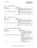
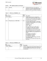
4
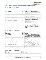
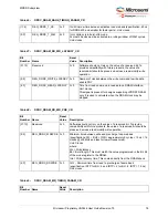
REG_DDRC_DIS_ACT_BYPASS
0×0
Only present in designs supporting activate bypass.
When 1, disable bypass path for high priority read
activates
3
REG_DDRC_DIS_RD_BYPASS
0×0
Only present in designs supporting read bypass.
When 1, disable bypass path for high priority read page
hits.
2
REG_DDRC_DIS_PRE_BYPASS
0×0
Only present in designs supporting precharge bypass.
When 1, disable bypass path for high priority
precharges
1
REG_DDRC_DIS_COLLISION_PAGE_OP
T
0×0
When this is set to ‘0’, auto-precharge is disabled for
the flushed command in a collision case. Collision
cases are write followed by read to same address, read
followed by write to same address, or write followed by
write to same address with REG_DDRC_DIS_WC bit =
1 (where same address comparisons exclude the two
address bits representing the critical word).
0
Reserved
0×0
Software should not rely on the value of a reserved bit.
To provide compatibility with future products, the value
of a reserved bit should be preserved across a read-
modify-write operation.
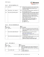
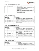
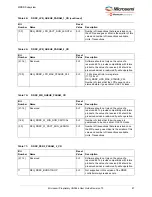
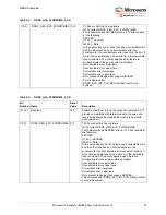
Table 57 •
DDRC_MODE_REG_RD_WR_CR
Bit
Number Name
Reset
Value Description
[31:4]
Reserved
0×0
Software should not rely on the value of a reserved bit. To provide
compatibility with future products, the value of a reserved bit should be
preserved across a read-modify-write operation.
3
REG_DDRC_MR_WR
0×0
When 1 is written and DDRC_REG_MR_WR_BUSY is Low, a mode
register read or write operation is started. There is no need for the CPU
to set this back to zero. This bit always reads as zero.
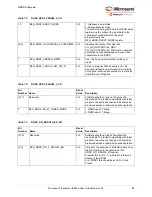
[2:1]
REG_DDRC_MR_ADDR
0×0
Address of the Mode register that is to be written to.
00: MR0
01: MR1
10: MR2
11: MR3
0
REG_DDRC_MR_TYPE
0×0
Indicates whether the Mode register operation is read or write.
1: Read
0: Write
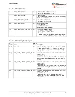
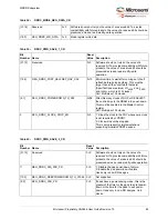
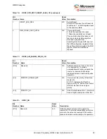
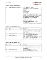
Table 58 •
DDRC_MODE_REG_DATA_CR
Bit
Number Name
Reset
Value Description
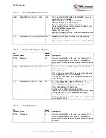
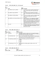
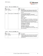
Table 56 •
DDRC_ADDR_MAP_COL_3_CR
(continued)
Bit
Numbe
r
Name
Reset
Value Description

