ISD94100 Series Technical Reference Manual
Sep 9, 2019
Page
244
of 928
Rev1.09
IS
D
9
410
0
S
ER
IE
S
T
E
C
HN
ICA
L
RE
F
E
RE
NCE
M
AN
U
AL
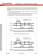
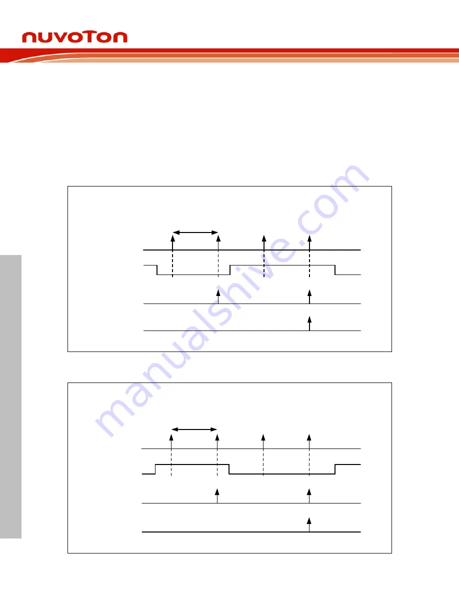
Figure 6.5-5 shows the triggering condition for a GPIO rising edge trigger interrupt. The interval of
time between the two valid sample signal is determined by DBCLKSRC (Px_DBCTL[4]) and
DBCLKSEL (Px_DBCTL[3:0]). Each valid data from GPIO pin need to be sampled twice. For rising
edge trigger:
if the pin status was low before DBEN (Px_DBEN) is enabled, an interrupt will be generated
when a valid high pin status is met.
If the pin status was high before DBEN (Px_DBEN) is enabled, an interrupt can only happen
after first a valid low status detected, and then a valid high status detected.
For falling edge trigger, the opposite triggering condition is shown in Figure 6.5-6.
Valid
sample
PA.0
(PA_PIN[0])
256*
(de-bounce
clock cycle)
PA_DBCTL[3:0] = 4'b1000
Valid
data
pin low
valid data
INTSRC[0]
(PA_INTSRC)
pin high
valid data
PA_INTYPE[0] = 1'b0
interrupt
Figure 6.5-5 GPIO Rising Edge Trigger Interrupt
Valid
sample
PA.0
(PA_PIN[0])
256*
(de-bounce
clock cycle)
PA_DBCTL[3:0] = 4'b1000
Valid
data
pin high
valid data
INTSRC[0]
(PA_INTSRC)
pin low
valid data
PA_INTYPE[0] = 1'b0
interrupt


