RTD Embedded Technologies, Inc.
| www.rtd.com
32
DM35418HR/DM35218HR
User’s Manual
BDM-610010041 Rev F
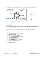
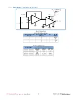
5.4.3.5. ADC Gain and Offset Test
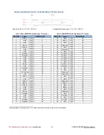
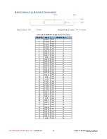
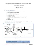
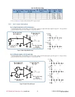
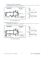
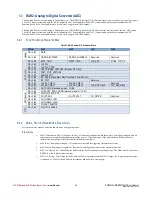
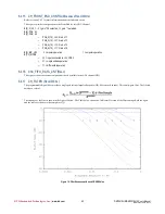
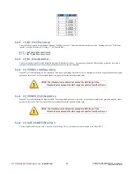
The following figure shows an example how to set up the FPGA registers to test the offset and gain of each channel. Figure 14 show the front end
and FPGA register settings for bipolar operation. Figure 14 show the front end and FPGA register settings for unipolar operation.
5.7
Analog output
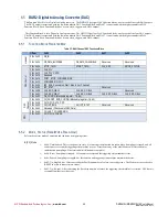
The DM35418HR/DM35218HR feature 4/8 independent 16-bit analog output channels with individually programmable output ranges of ±2.5V,
±5V, and ±10V. Each channel supports a maximum update rate 1 MHz and a maximum operating load of 5mA. Each channel has less than 1 Ω of
output impedance.
Each DAC converter has a 511 sample FIFO for DMA. Each sample is packed into 32 bits, right justified and sign-extended.
5.7.1
I
NITIALIZING THE
DAC
C
ONVERTER
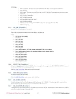
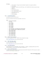
The following is a list of the typical steps needed to initialize the DAC converter and begin sampling:
1.
Set the DAC to the Uninitialized state (MODE = Uninitialized)
2.
Setup the DMA for the channel
3.
Set the input mode (CH_FRONT_END_CONFIG)
4.
Set the start and stop triggers (START_TRIG, STOP_TRIG)
5.
Set the clock source (CLK_SOURCE)
6.
Set the sample rate (CLK_DIV_CNTR)
7.
Set the Post Capture counter (POST_STOP_CAPTURE)
8.
Set the DAC to the Reset state (MODE = Reset)
9.
Start the DMA
10.
Start the DAC (MODE = Go)
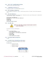
Figure 14: Bipolar Offset and Gain Test Circuit
+
-
VREF
CHn_Front_End_Config
[PGA_A[1:0]]
G=1
:
0, 0
+15V
-15V
IN+
IN-
A1 A0 -> G
Gain
CHn_Front_End_Config
[BIP_UNI]
VREF: 0V: [BIP_UNI] = 0
X
CHn_Front_End_Config
[VREF_NORMAL] = 0
CHn_Front_End_Config
[SE_DIFF] = 0
U
PGA
X
+5V
t
10V
U
PGA
(t)
-10V
5V


