background image

RTC – 4553AC


CONTETS 


1. Overview..........................................................................................1


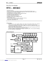
2. Block Diagram .................................................................................1


3. Terminal description ........................................................................2


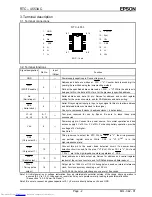
3.1. Terminal connections ........................................................................................ 2


3.2. Terminal functions............................................................................................. 2


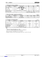
4. Absolute maximum ratings...............................................................3


5. Recommended operating conditions................................................3


6. Frequency characteristics ................................................................3


7. Electrical characteristics ..................................................................4


7.1. DC, AC Characteristics ..................................................................................... 4


7.1.1. V

DD

 = 5 V........................................................................................................................... 4


7.1.2. V

DD

 = 3 V........................................................................................................................... 5


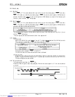
7.2. Timing Chart ..................................................................................................... 6


8. How to use.......................................................................................7


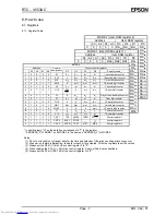
8.1. Registers........................................................................................................... 7


8.1.1. Register Table ................................................................................................................... 7


8.1.2. Register Bit Functions ....................................................................................................... 8


8.2. Register Description.......................................................................................... 9


8.2.1. Time/Calendar Counter Registers ..................................................................................... 9


8.2.2. Control Registers ............................................................................................................. 10


8.3. How to use ...................................................................................................... 12


8.3.1. Data Read ....................................................................................................................... 12


8.3.2. Data Write/Modify ............................................................................................................ 12


8.3.3. Initialize............................................................................................................................ 12


8.3.4. Timing Pulse Output ........................................................................................................ 12


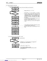
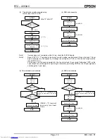
8.3.5. Sample Operation Flow Charts........................................................................................ 13


8.3.6. CS1 and CS0 Operation................................................................................................. 15


8.3.7. System Power Down During Interface Operation ............................................................ 15


8.3.8. Power Supply and CS1 Operation ................................................................................... 15


8.3.9. Power-On Reset .............................................................................................................. 16


8.3.10. Power Supply Connection Example .............................................................................. 16


8.3.11. Processing of Non-Existent Data................................................................................... 17


8.3.12. Timing Charts ................................................................................................................ 18


9. External dimensions / Marking layout ............................................21


9.1. External dimensions........................................................................................ 21


9.2. Marking layout................................................................................................. 21


10. Reference Data ...........................................................................22


11. Application notes .........................................................................23


11.1. Notes on handling ......................................................................................... 23


11.2. Notes on packaging ...................................................................................... 23


Downloaded from 

Elcodis.com


electronic components distributor


Summary of Contents for RTC-4553AC

Page 1: ...MQ342 01 Application Manual Real Time Clock Module RTC 4553AC Downloaded from Elcodis com electronic components distributor...

Page 2: ...granted by implication or otherwise and there is no representation or warranty that anything made in accordance with this material will be free from any patent or copyright infringement of a third par...

Page 3: ...8 2 2 Control Registers 10 8 3 How to use 12 8 3 1 Data Read 12 8 3 2 Data Write Modify 12 8 3 3 Initialize 12 8 3 4 Timing Pulse Output 12 8 3 5 Sample Operation Flow Charts 13 8 3 6 CS1 and CS0 Ope...

Page 4: ...s a very compact real time clock module with permanent calendar and serial data input output The module is designed for E mater time accuracy is within 5 10 6 0 432 sec day It incorporates a heat resi...

Page 5: ...For normal operation and bus access supply 5 V 10 or 3 V 10 For backup battery operation provide a voltage of 2 V or higher See Note 1 CS0 Chip select 0 11 I This pin serves to select the RTC While C...

Page 6: ...emperature TOPR No condensation 30 70 C 6 Frequency characteristics GND 0 V Item Symbol Condition Rating Unit 5 10 6 Frequency precision f fo Ta 25 C VDD 5 0 V AC 0 432 sec day Frequency temperature c...

Page 7: ...N 0 V 2 0 2 0 A Oscillation startup time Ts Ta 25 C 3 0 s 2 AC Characteristics GND 0 V Ta 30 C 70 C VDD 5 V 10 Item Symbol Condition Min Typ Max Unit SCK frequency fCLK 500 kHz SCK L time tWCKL 1 0 SC...

Page 8: ...startup time TS Ta 25 C 3 0 s 2 AC Characteristics GND 0 V Ta 30 C 70 C VDD 3 V 10 Item Symbol Condition Min Typ Max Unit SCK frequency fCLK 300 kHz SCK L time tWCKL 1 5 SCK H time tWCKH 1 5 SCK paus...

Page 9: ...tps tDSO 90 1 8 1 10 10 90 10 tDPZ2 tDPZ1 90 90 10 90 90 90 90 10 10 10 10 tSWR tHWR tDSZ2 tHCS tWCKH tWCKL tSCS 1 f CLK tHD tSD tDSZ1 CS0 SCK SIN WR SOUT CS0 SCK SCK SOUT CS1 TPOUT Downloaded from E...

Page 10: ...A1 A0 D3 D2 D1 D0 0 0 0 0 0 RA3 RA2 RA1 RA0 RA4 RA8 RA12 RA16 RA20 RA24 RA28 RA32 RA36 RA40 RA44 RA48 RA52 RA56 MS0 MODE 0 Address Counter control register A3 A2 A1 A0 Register designation D3 D2 D1 D0...

Page 11: ...de Meaning 0 No carry Time calendar counter read write possible 1 Carry Time calendar counter read write prohibited PONC Power on clear detection At power on the power on clear function automatically...

Page 12: ...24 hour format is switched during clock operation 4 Day of the week digit counter A3 A2 A1 A0 Name D3 D2 D1 D0 Register contents 0 1 1 0 W 0 w4 w2 w1 Day of the week digit counter Counts values from...

Page 13: ...s written to the 30ADJ bit the bit automatically resets itself to 0 within 76 3 s The 30 second adjustment function also resets fractions below full seconds The TPOUT 1 10 Hz duty changes for one cycl...

Page 14: ...bit is the power on clear detection bit see next page It is set to 1 when power on clear is detected The PONC bit is reset 1 0 by setting the SYSR bit to 1 c D1 bit bit marked When this bit is read da...

Page 15: ...ounter can be incremented via the 1 hour digit counter 8 3 3 Initialize 1 System reset When the SYSR bit in the control register 3 is set to 1 all logic bits are initialized The SYSR bit is reset to 0...

Page 16: ...e BUSY bit down transition was detected If the process takes longer the BUSY bit must be checked again for continued processing It is advisable to start the setting from the year digit to prevent sett...

Page 17: ...00 to 2 00 the hour digit must be reset CNTR 1 For the year CNTR is used separately for the 1 year digit and 10 year digit Performing CNTR on the 1 year digit does not change the 10 year digit Conver...

Page 18: ...rcuits To internal circuits To internal circuits From internal circuits From internal circuits CS1 CS0 WR SCK SIN SOUT TPOUT 8 3 7 System Power Down During Interface Operation When the system power go...

Page 19: ...t may not be performed correctly Be sure to verify correct operation Note 2 Within the voltage range for data retention and clock operation 2 0 V 5 5 V power on reset is designed not to be performed u...

Page 20: ...mented Carry from hour digit Feb 29 00 Feb 29 01 Mar 01 01 When the following non existent data are set February 30 incrementing the 10 day digit causes an overflow in the 10 day digit clearing the 1...

Page 21: ...and data Data Address 10 second digit contents Data Address 1 second digit contents Data WR CSo SCK Don t care SIN Undefined SOUT When specifying the next data read access the previously accessed add...

Page 22: ...ted by 1 For continuous write operations the CS0 must be kept L for the required number of increments 1 SIN Input at leading edge of SCK SOUT Output at trailing edge of SCK 4 SRAM data write example d...

Page 23: ...rementing steps Data after incrementing 0 4 4 8 3 11 10 digit is carried automatically Control register and SRAM Address and 4 bit data are written The selected counter register or RAM address data ar...

Page 24: ...7 4 0 2 14 8 7 1 1 4 1 4 5 4 1 27 1 27 6 7 62 0 7 Unit mm 9 2 Marking layout RTC 4553AC SOP 14pin Symbol mark Frequency tolerance indication Indication Frequency tolerance AC 5 10 6 Model identifier...

Page 25: ...e fT Frequency deviation at given temperature fV Frequency deviation at given voltage 3 Calculating the daily deviation Daily deviation f f 86400 seconds For example at f f 11 574 10 6 the deviation i...

Page 26: ...lfunctions due to noise Therefore pull up or pull down resistors should be provided for all unused input pins except L1 L5 pins 11 2 Notes on packaging 1 Soldering temperature conditions If the temper...

Page 27: ...01 FRANCE FRENCH Branch Office 1 Avenue de l Atlantique LP 915 Les Conquerants Z A de Courtaboeuf 2 F 91976 Les Ulis Cedex France Phone 33 0 1 64862350 Fax 33 0 1 64862355 ASIA CHINA EPSON CHINA CO LT...

Reviews: