Copyright © Siemens AG 2016. All rights reserved
370
ERTEC 200P-2 Manual
Technical data subject to change
Version 1.0
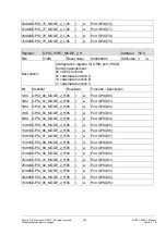
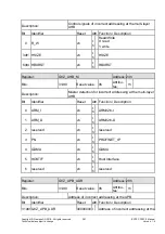
With LOCAL_OUT_READ_L and LOCAL_OUT_READ_H, you can configure whether the
value of the GPIO block or of the data IO value is returned for GPIOs 32…95 (see
2.3.10.8.4.2).
To adapt the interrupt-compatible GPIOs 0...15 to an external circuit that supplies both
low-active and high-active signals, they can be connected to the following modules over
GPIO_INT_POLSEL either unchanged (not inverted) or inverted:
ARM-ICU (GPIO0…15 IRQ32..47, see 2.3.2.14)
PN-ICU1 (GPIO4…7, see 2.3.8.1.2)
GDMA (GPIO0…3 HW jobs 16...19, see 2.3.4.2.1.1)
.
POLSEL_GPIOx must be configured to ensure that these modules always receive
a high-active signal.
The value in the GPIO_IN_0 register is also saved unchanged or
inverted from the the input signal.
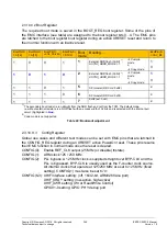
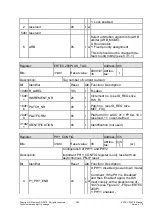
2.3.10.9.12 I²C Clock Divider
The bit rate of the I
2
C bus is configured with the CCR_I2C register. I
2
C transmission rates
of 100 kb/s max require a 1 MHz enable for I
2
C-IP (MI2C: Inventra). This enable is im-
plemented in
CCR_I2C.CDIV_VAL
configuration. The value to be configured is calculated
using the following formula:
CLK [MHz] / (ClockDivider + 1) = 1 MHz
with a 125 MHz system clock
CDIV_VAL
= 0x7C (Default)
Important:
A max. transmission rate of 100 kb/s is supported.
2.3.10.9.13 EDC Register
The EDC logic for D-TCM in ARM926 can be enabled and disabled in the EDC register
EDC_PARITY_EN. The parity logic for the I and D cache for ARM926 can also be acti-
vated.
One-bit and multi-bit errors for all EDC-protected RAM are saved in EDC_EVENT and the
corresponding level-triggered interrupt event
EDC_Event
(IRQ48) triggered in ARM-ICU
(see 2.3.2.14). The register bits (i.e. the active interrupt level) can only be reset with write
access by the FW (writing a '0').
Note: The register bits can also be set by the FW for debugging with write access (writing
a '1').
If a one-bit or multi-bit error is saved at the same time as the FW deletes the error with
write access, the one-bit or multi-bit error will not be deleted.
The end of RAM initialization (INIT_DONE) for all EDC-protected RAM is signaled in
EDC_INIT_DONE.
2.3.10.9.14 ARM926 Mapping
The partitioning of ARM926 subsystem TCM into I-TCM and D-TCM can be configured in
steps of 64 KByte in TCM926_MAP.
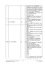
2.3.10.9.15 PAD Control Register
The IO buffers at the XHIF / GPIO interface support both 3.3 V and 1.8 V IO. The IO
buffers of the EMC interface are designed for an IO voltage of 1.8 V. The
driver power
of

