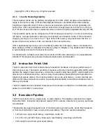
MSEL
Reset address
Purpose
00
0x0000_1004
loops forever waiting for debugger
01
0x2000_0000
memory-mapped QSPI0
10
0x0002_0000
memory-mapped OTP
11
0x0001_0000
memory-mapped Mask ROM (jumps to OTP)
Table 7:
Target of the reset vector
MROM is fixed at design time, and is located on the peripheral bus on FE310-G002, but instruc-
tions fetched from MROM are cached by the core’s I-cache. The MROM contains an instruction
at address
0x1_0000
which jumps to the OTP start address at
0x2_0000
.
One-Time Programmable (OTP) Memory
The OTP is located on the peripheral bus, with both a control register interface to program the
OTP, and a memory read port interface to fetch words from the OTP. Instruction fetches from the
OTP memory read port are cached in the E31 core’s instruction cache.
The OTP needs to be programmed before use and can only be programmed by code running
on the core. The OTP bits contain all 0s prior to programming.
Quad SPI Flash Controller (QSPI)
The dedicated QSPI flash controller connects to external SPI flash devices that are used for
execute-in-place code. SPI flash is not available in certain scenarios such as package testing or
board designs not using SPI flash (e.g., just using on-chip OTP).
Off-chip SPI devices can vary in number of supported I/O bits (1, 2, or 4). SPI flash bits contain
all 1s prior to programming.
Copyright © 2019, SiFive Inc. All rights reserved.
24
Summary of Contents for FE310-G002
Page 1: ...SiFive FE310 G002 Manual v19p05 SiFive Inc ...
Page 11: ...Figure 1 FE310 G002 top level block diagram Copyright 2019 SiFive Inc All rights reserved 9 ...
Page 15: ...Chapter 2 List of Abbreviations and Terms 13 ...
Page 23: ...Chapter 4 Memory Map The memory map of the FE310 G002 is shown in Table 4 21 ...

