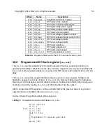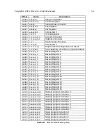
Offset
Name
Description
0x00
otp_lock
Programmed-I/O lock register
0x04
otp_ck
OTP device clock signals
0x08
otp_oe
OTP device output-enable signal
0x0C
otp_sel
OTP device chip-select signal
0x10
otp_we
OTP device write-enable signal
0x14
otp_mr
OTP device mode register
0x18
otp_mrr
OTP read-voltage regulator control
0x1C
otp_mpp
OTP write-voltage charge pump control
0x20
otp_vrren
OTP read-voltage enable
0x24
otp_vppen
OTP write-voltage enable
0x28
otp_a
OTP device address
0x2C
otp_d
OTP device data input
0x30
otp_q
OTP device data output
0x34
otp_rsctrl
OTP read sequencer control
Programmed-I/O lock register (
The
otp_lock
register supports synchronization between the read sequencer and the pro-
grammed-I/O interface. When the lock is clear, memory-mapped reads may proceed. When the
lock is set, memory-mapped reads do not access the OTP device, and instead return
0
immedi-
ately.
The
otp_lock
should be acquired before writing to any other control register. Software can
attempt to acquire the lock by storing
1
to
otp_lock
. If a memory-mapped read is in progress,
the lock will not be acquired, and will retain the value
0
. Software can check if the lock was suc-
cessfully acquired by loading
otp_lock
and checking that it has the value
1
.
After a programmed-I/O sequence, software should restore the previous value of any control
registers that were modified, then store
0
to
otp_lock
.
Listing 1 shows the synchronization code sequence.
Listing 1:
Sequence to acquire and release
otp_lock
.
la t0, otp_lock
li t1, 1
loop: sw t1, (t0)
lw t2, (t0)
beqz t2, loop
#
# Programmed I/O sequence goes here.
#
sw x0, (t0)
Table 34:
Register offsets within the OTP Controller memory map
Copyright © 2019, SiFive Inc. All rights reserved.
53
Summary of Contents for FE310-G002
Page 1: ...SiFive FE310 G002 Manual v19p05 SiFive Inc ...
Page 11: ...Figure 1 FE310 G002 top level block diagram Copyright 2019 SiFive Inc All rights reserved 9 ...
Page 15: ...Chapter 2 List of Abbreviations and Terms 13 ...
Page 23: ...Chapter 4 Memory Map The memory map of the FE310 G002 is shown in Table 4 21 ...


