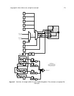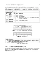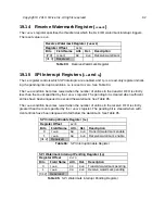
A single interrupt bit can be generated for each GPIO bit. The interrupt can be driven by rising
or falling edges, or by level values, and interrupts can be enabled for each GPIO bit individually.
Inputs are synchronized before being sampled by the interrupt logic, so the input pulse width
must be long enough to be detected by the synchronization logic.
To enable an interrupt, set the corresponding bit in the
rise_ie
and/or
fall_ie
to
1
. If the cor-
responding bit in
rise_ip
or
fall_ip
is set, an interrupt pin is raised.
Once the interrupt is pending, it will remain set until a
1
is written to the
*_ip
register at that bit.
The interrupt pins may be routed to the PLIC or directly to local interrupts.
When configured as inputs, each pin has an internal pull-up which can be enabled by software.
At reset, all pins are set as inputs, and pull-ups are disabled.
When configured as output, each pin has a software-controllable drive strength.
When configured as an output (either software or IOF controlled), the software-writable
out_xor
register is combined with the output to invert it.
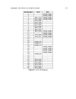
Each GPIO pin can implement up to 2 HW-Driven functions (IOF) enabled with the
iof_en
reg-
ister. Which IOF is used is selected with the
iof_sel
register.
When a pin is set to perform an IOF, it is possible that the software registers
port
,
output_en
,
pullup
,
ds
,
input_en
may not be used to control the pin directly. Rather, the pins may be con-
trolled by hardware driving the IOF. Which functionalities are controlled by the IOF and which
are controlled by the software registers are fixed in the hardware on a per-IOF basis. Those that
are not controlled by the hardware continue to be controlled by the software registers.
If there is no IOFx for a pin configured with IOFx, the pin reverts to full software control.
Copyright © 2019, SiFive Inc. All rights reserved.
77
Summary of Contents for FE310-G002
Page 1: ...SiFive FE310 G002 Manual v19p05 SiFive Inc ...
Page 11: ...Figure 1 FE310 G002 top level block diagram Copyright 2019 SiFive Inc All rights reserved 9 ...
Page 15: ...Chapter 2 List of Abbreviations and Terms 13 ...
Page 23: ...Chapter 4 Memory Map The memory map of the FE310 G002 is shown in Table 4 21 ...

