


EVK-IRIS-W10 - User guide
UBX-23007837 - R03
Hardware description
Page 26 of 43
C1-Public
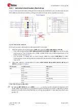
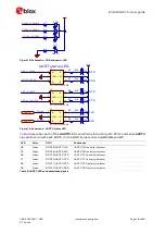
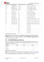
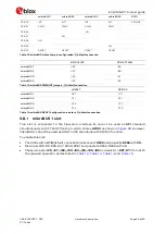
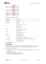
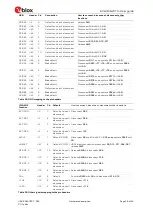
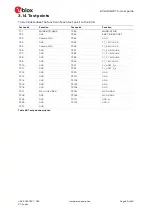
mikroBUS 1
mikroBUS 2
mikroBUS 3
mikroBUS 4
SDIO
GPIO18
INT
INT*
INT
INT
SDIO-D2
GPIO27
PWM
PWM*
PWM
PWM
GPIO46
AN
GPIO47
AN
GPIO48
AN
GPIO49
AN
GPIO50
RESET
RESET
RESET
RESET
Table 12: mikroBUS slots other pin configuration, (*) default connection
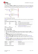
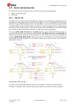
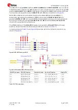
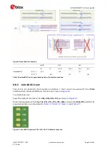
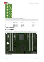
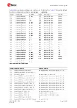
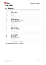
GPIO 18 INT
GPIO 27 PWM
mikroBUS 1
J92
J89
mikroBUS 2
J91*
J88*
mikroBUS 3
J62
J61
mikroBUS 4
J93
J90
Table 13: mikroBUS PWM/INT jumpers, (*) default connection
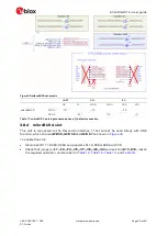
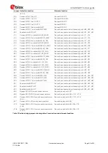
nRESET
GPIO 50
mikroBUS 1
R67
R71
mikroBUS 2
R11
R21
mikroBUS 3
R46
R70
mikroBUS 4
R10
R19
Table 14: mikroBUS RESET configuration resistors, (*) default connection
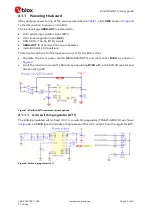
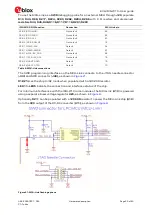
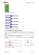
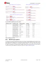
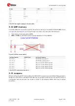
3.8.1
mikroBUS 1 slot
This slot is connected to the Flexcomm interface
0
, cannot be used as
SPI
standard
simultaneously with FTDI-SPI function, which shares
GPIO4
. However,
mikroBUS1 can still be used as UART or I2C standards with 2WCI-2 function.
To enable this slot:
•
The USB switch
U18
(default connection)
disconnect
R255
and populate
R256
with
0R.
•
Disconnect R8, R9, R38, R37, R259, R261 and populate R260, R262 with 0R.
•
Check jumpers
J25, J27, J80, J83, J84, J85, J89, J92
and resistors
R67, R71
to match
the required operation, as described in
and