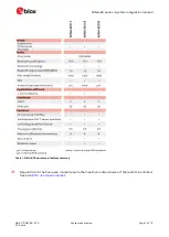
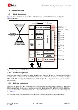
background image


UBX-17056748 - R13 

C1-Public 


www.u-blox.com


NINA-B3 series


Stand-alone Bluetooth 5 low energy modules 

System integration manual 


Abstract


This document describes the system integration of the NINA-B3 series stand-alone Bluetooth 5 low 
energy modules. 


Summary of Contents for NINA-B3 Series

Page 1: ...lic www u blox com NINA B3 series Stand alone Bluetooth 5 low energy modules System integration manual Abstract This document describes the system integration of the NINA B3 series stand alone Bluetoo...

Page 2: ...Production Information NINA B302 Early Production Information NINA B306 Early Production Information NINA B306 01B is without external LFXO u connectXpress Product name Document status Comment NINA B3...

Page 3: ...sensor 10 1 6 Debug Serial Wire Debug SWD 10 1 7 Serial interfaces 10 1 7 1 Universal Asynchronous Serial Interface UART 10 1 7 2 Serial Peripheral Interface SPI 11 1 7 3 Quad serial peripheral interf...

Page 4: ...C interface 40 3 6 1 Battery protection 41 3 7 General High Speed layout guidelines 41 3 7 1 General considerations for schematic design and PCB floor planning 41 3 7 2 Module placement 42 3 7 3 Layou...

Page 5: ...ct labelling requirement 55 5 5 KCC South Korean market 56 5 5 1 Compliance statement 56 5 5 2 End product labeling requirements 56 5 5 3 End product user manual requirements 57 5 6 Anatel Brazil comp...

Page 6: ...at enable customer applications to run on the built in Arm Cortex M4 with FPU With 1 MB flash and 256 kB RAM they offer the best in class capacity for customer applications on top of the Bluetooth low...

Page 7: ...anual UBX 17056748 R13 System description Page 7 of 72 C1 Public Table 1 NINA B30 series main features summary Regulations in the European market require the maximum output power of the radio to be li...

Page 8: ...NINA B3 can be used either together with the pre flashed u connectXpress software or as an open CPU module where you can run your own application developed with the Nordic SDK development environment...

Page 9: ...4 2 Digital I O interfaces reference voltage VCC_IO On NINA B3 series modules the I O voltage level is the same as the supply voltage and VCC_IO is internally connected to the supply input VCC When u...

Page 10: ...es an external or hardware reset of the module The current parameter settings are not saved in the non volatile memory of the module and a proper network detach is not performed 1 5 2 Internal tempera...

Page 11: ...pgrade The I O level of the UART will follow the VCC voltage and it can thus be in the range of 1 8 V and 3 6 V If you are connecting the NINA B3 module to a host with a different voltage on the UART...

Page 12: ...state NINA B3 modules have 38 GPIO pins and no analog or digital interfaces All interfaces or functions must be allocated to a GPIO pin before use Eight of the 38 GPIO pins are analog enabled meaning...

Page 13: ...ain a higher effective resolution Continuous sampling can be configured to sample at a configurable time interval or at different internal or external events without CPU involvement Table 5 Acquisitio...

Page 14: ...hile using an external antenna the PCB to RF cable transition must be implemented using either a suitable 50 connector or an RF signal solder pad including GND that is optimized for 50 characteristic...

Page 15: ...modules include a Near Field Communication interface capable of operating as a 13 56 MHz NFC tag at a bit rate of 106 kbps As an NFC tag data can be read from or written to the NINA B3 modules using a...

Page 16: ...ecure boot loader and pre flashed u connectXpress software The u connectXpress software enables use of the Bluetooth Low Energy functions controlled by AT commands over the UART interface Some of the...

Page 17: ...ware development kit documentation available at the Nordic Semiconductor Infocenter 14 The easiest way to get started with the Nordic SDK is to copy one of the examples in the SDK Choose an example th...

Page 18: ...gnal pin define ARDUINO_13_PIN NRF_GPIO_PIN_MAP 0 7 define ARDUINO_12_PIN NRF_GPIO_PIN_MAP 0 2 define ARDUINO_11_PIN NRF_GPIO_PIN_MAP 0 15 define ARDUINO_10_PIN NRF_GPIO_PIN_MAP 0 14 define ARDUINO_9_...

Page 19: ...ASPBERRY_PI_24_PIN NRF_GPIO_PIN_MAP 0 27 define RASPBERRY_PI_26_PIN NRF_GPIO_PIN_MAP 0 6 define RASPBERRY_PI_28_PIN NRF_GPIO_PIN_MAP 1 14 define RASPBERRY_PI_32_PIN NRF_GPIO_PIN_MAP 1 10 define RASPBE...

Page 20: ...figuration in the Segger Studio project Figure 4 Add a build configuration to Segger Studio 2 Configure the build configuration to use your board definition Assuming that you are basing your project o...

Page 21: ...RF Connect for Desktop application and from there install the nRF Connect SDK For more information see reference 23 2 If a command line environment is preferred see the Getting Started section on the...

Page 22: ...cumentation 21 2 2 3 Saving Bluetooth MAC address and other production data Open CPU B30x variants of the NINA B3 module come with a pre programmed Bluetooth MAC address If needed this address can be...

Page 23: ...el software description file name version flash address image size image id file permissions and signature file reference for the SoftDevice and ConnectivitySoftware applications Java Script Object No...

Page 24: ...he serial interface using open source terminal emulator software that supports XMODEM like TeraTerm or ExtraPuTTy Alternatively you can send all AT commands described in this section using the s cente...

Page 25: ...X SW 3 0 0 005 Address 0x26000 Size 0x4C95C Id 0x0 Permissions rwx SignatureFile NINA B31X SI 3 0 0 005 txt Label SoftDevice Description S140 softdevice from Nordic for NINA NRF File NINA S140 SD 6 1...

Page 26: ...re marked in UNIX style rwx is the default flag for the u connectXpress software rw is the default flag for other binary images Table 7 Defined values for update parameters 2 3 1 2 1 Setting up the se...

Page 27: ...ess software AT GMR 2 0 0 025 OK 3 Prepare the module to accept a binary file for download and start the bootloader at the appropriate baud rate Enter the Update software AT UFWUPD command together wi...

Page 28: ...an send AT text commands to NINA B3 to execute tasks using open source terminal emulator software that supports XMODEM like TeraTerm or ExtraPuTTy Alternatively you can send all AT commands described...

Page 29: ...sVpgv670y8FwH8LYFANspk5Yl DfOXwFcgqWKcHmN0lcKAt4b2ug u BItwsoQpbzwDnWLUwDJBIa6ZgsdLx kTUNW3hWdGvQuFIfwXk4NhvX 3RlIOmPqM shkN7tF4kaSeS aUp Ub81edKC57kQa8L0uWXVhRyI3OwoGkvXBMKoKVIphFgP6WwKdwanrI6TWID5I...

Page 30: ...file transfer using XMODEM protocol Enter the configuration action command x with the ConnectivitySoftware values imageaddress imagesize imagename permissions and imageid defined in the NINA B31X CF...

Page 31: ...external debugger SEGGER J Link BASE works with the NINA B30 modules The EVK NINA B30 evaluation kit incorporates an onboard debugger and can therefore be flashed without any external debugger See als...

Page 32: ...w the NINA B3x6 PCB trace antenna and Asynchronous serial interface UART design guidelines 5 System functions RESET_N I2C GPIO and other System input and output pins Accurate design is required to ens...

Page 33: ...trip track coupled to ground plane and side conductors separated by dielectric materials Strip track sandwiched between two parallel ground planes and separated by dielectric materials Figure 10 Trans...

Page 34: ...yer Route RF transmission lines far from any noise source as switching supplies and digital lines and from any sensitive circuit to avoid crosstalk between RF traces and Hi impedance or analog signals...

Page 35: ...tion should be considered if possible to maximize the performance and fulfill the requirements in Table 8 As a numerical example the physical restriction to the PCB design can be considered as shown b...

Page 36: ...Hirose U FL Ultra Small Surface Mount Coaxial Connector Recommended I PEX MHF Micro Coaxial Connector Tyco UMCC Ultra Miniature Coax Connector Amphenol RF AMC Amphenol Micro Coaxial Lighthorse Techno...

Page 37: ...acement of the antenna and its surroundings is also critical for antenna performance Avoid placing the antenna close to conductive or RF absorbing parts such as metal objects ferrite sheets and so on...

Page 38: ...ch a way that the antenna is not subject to physical force NINA B3x6 PCB trace antenna The module shall be placed in the center of an edge of the host PCB A large ground plane on the host PCB is a pre...

Page 39: ...ect RF performance a good connection of the module VCC pin with DC supply source is necessary Guidelines for the supply design are summarized below The VCC connection must be as wide and short as poss...

Page 40: ...ule applies a 0 ON state low level when it is ready to receive transmission 3 5 2 Serial peripheral interface SPI The layout of the SPI bus should be made so that noise injection and cross talk are av...

Page 41: ...between the battery and the device in order to protect the battery 3 7 General High Speed layout guidelines These general design guidelines are considered as best practices and are valid for any bus...

Page 42: ...on the board Ground splitting is not allowed below the module Minimize the bus length to reduce potential EMI issues from digital buses All traces including low speed or DC traces must couple with a r...

Page 43: ...nt and its interconnecting cable surfaces The applicability of ESD immunity test to the whole device depends on the device classification as defined by ETSI EN 301 489 1 Applicability of the ESD immun...

Page 44: ...not touch any charged capacitors Be especially careful when handling materials like patch antennas 10 pF coaxial cables 50 80 pF m soldering irons or any other materials that can develop charges To pr...

Page 45: ...l mass of the entire populated PCB the heat transfer efficiency of the oven and the type of solder paste that is used The optimal soldering profile that is used must be trimmed for each case depending...

Page 46: ...ds with a module populated on them Boards with combined through hole THT components and surface mounted SMT devices may require wave soldering Only a single wave soldering process is allowed for board...

Page 47: ...vailable in the NINA B3 Declaration of Conformity 15 Module integrators are required to make their own Declaration of Conformity in which test standards and directives that are tested and fulfilled by...

Page 48: ...n of the transmit antenna must be considered for the EIRP calculation Implementation in the NINA B31 series In the u connectXpress software output power can be configured by using the Bluetooth config...

Page 49: ...antenna Increase the separation between the equipment and receiver Connect the equipment into an outlet on a circuit different from that to which the receiver is connected Consult the dealer or an exp...

Page 50: ...tted in the FCC restricted band starting at 2483 5 MHz As a result channel 26 must not be used on the US Canadian market Implementation in NINA B31 series IEEE 802 15 4 is currently not supported in t...

Page 51: ...nic of 2 4 GHz as declared in 47 CFR Part 15 33 b 1 The following requirements apply to all products that integrate a radio module Subpart B UNINTENTIONAL RADIATORS To verify that the composite device...

Page 52: ...s y trouvent L tiquette d homologation d un module d Innovation Sciences et D veloppement conomique Canada devra tre pos e sur le produit h te un endroit bien en vue en tout temps En l absence d tiqu...

Page 53: ...pareils radio exempts de licence L exploitation est autoris e aux deux conditions suivantes 1 l appareil ne doit pas produire de brouillage 2 l utilisateur de l appareil doit accepter tout brouillage...

Page 54: ...esponsibility to make sure that the protocol uses at least 48 bit addressing Failure to comply with these requirements will void the NINA B3 Japan certification and it will be illegal to place the end...

Page 55: ...low power radio frequency devices must be susceptible with the interference from legal communications or ISM radio wave radiated devices 5 4 2 End product labelling requirement When a product integrat...

Page 56: ...LP197AT6 NINA B306 CCAI19LP1670T0 NINA B311 CCAI18LP197BT8 NINA B312 CCAI18LP197CT0 NINA B316 CCAI19LP1680T3 Table 13 NINA B3 series NCC ID certification numbers 5 5 KCC South Korean market 5 5 1 Comp...

Page 57: ...ormation shall be placed in a prominent location in the instruction manual or pamphlet supplied to the user or alternatively shall be placed on the container in which the device is marketed In case wh...

Page 58: ...the following website Independent Communications Authority of South Africa ICASA web site https www icasa org za 5 9 Integration checklist The following checklist can be used to get an overview of th...

Page 59: ...s are fulfilled Specific to the South Korean market The end product labelling requirements are fulfilled The end product user manual requirements are fulfilled Specific to the Brazilian market The end...

Page 60: ...e minimum cable loss to meet the regulatory requirements Minimum cable length 100 mm Comment The Reverse Polarity SMA connector can be mounted in a panel For information about integrating the U FL con...

Page 61: ...everse Polarity SMA adapter cable An SMA version antenna is also available but not recommended for use Ex IT 2400 SMA 28 001 Approval FCC IC RED MIC NCC KCC ANATEL ACMA and ICASA Original part number...

Page 62: ...deTM 2400 Manufacturer ProAnt Gain 3 0 dBi Impedance 50 Size 27 x 12 mm triangular Type Patch Cable length 100 mm Connector U FL connector Comment Should be attached to a plastic enclosure or part for...

Page 63: ...est report for each unit can be generated Figure 29 shows the ATE typically used during u blox production u blox in line production testing includes Digital self tests firmware download MAC address pr...

Page 64: ...cuit if the test result deviates that from that taken against a Golden Device The standard operational module firmware and test software on the host can be used to perform functional tests communicati...

Page 65: ...Emitting Diode LFXO Low Frequency Crystal Oscillator MAC Media access control MISO Master input slave output MOSI Master output slave input MSL Moisture sensitivity level NFC Near Field Communication...

Page 66: ...s IoT smart home automation devices to communicate on a local wireless mesh network THT Through Hole Technology TXD Transmit data UART Universal asynchronous receiver transmitter UICR User information...

Page 67: ...g PCB layout must be identical to the one provided by u blox Implement one of the reference designs described in this section or contact u blox The designer must use the PCB stack up provided by u blo...

Page 68: ...coplanar microstrip matched to 50 5 GND trace Minimum required top layer GND trace See also Figure 33 6 Copper keep out Keep this area free from any copper on the top layer Table 15 Included parts in...

Page 69: ...n Table 16 the increased spacing to GND does not affect the trace impedance significantly for short trace lengths Therefore the impedance will still be close to 50 Figure 33 RF trace and minimum requi...

Page 70: ...N 60950 1 2006 Information technology equipment Safety Part 1 General requirements 12 FCC Regulatory Information Title 47 Telecommunication 13 JESD51 Overview of methodology for thermal testing of sin...

Page 71: ...19 fbro Updated u connectScript version to 1 0 1 and modified the product status for NINA B31x 20B to Initial Production Included information about Bluetooth MAC address section 2 2 3 Corrected inform...

Page 72: ...ox com Regional Office China Beijing Phone 86 10 68 133 545 E mail info_cn u blox com Support support_cn u blox com Regional Office China Chongqing Phone 86 23 6815 1588 E mail info_cn u blox com Supp...

Reviews: