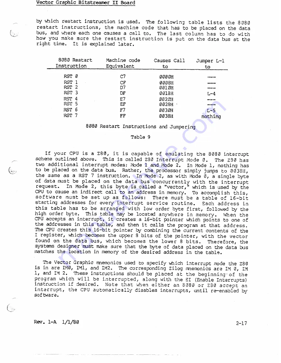
background image

by \vhich restart

instruction

is used.

The

followin;

table

lists

the

8380

restart

instructions,

the

machine

code

that has

to be placed

on

the data

bus,

and \vhere each one causes

a call

to.

The

last

colu~n

has

to do

with

how

you

make

sure

the

restart

instruction

is put

on the data

bus at the

right

time.

It is explained

later.

8080

Restart

Machine

code

Causes

Call

Instruction

Equivalent

to

RST

10

C7

0000H

RST

I

CF

eJI0108B

RST 2

D7

0010H

RST3

OF

0018H

RST 4

E7

0020H

RST 5

EF

10028H

RST 6

F7

0030H

RST 7

FF

0038H

Jumper

L-l

to

L-S

nothi~

If your

CPU

is a Z80, it

is capable

of

emulating

the

8080 interrupt

schene

outlined

above.

This

is called

ZS0 Interrupt

Mode

0.

The

230 has

two

additional

interrupt

modes:

r~de

1 and (~de

2.

In Mode

1, nothing

has

to be placed

on the data

oos.

Rather,

the processor

simply

jumps

to

003811,

the

same

as a RST

7 instruction.

In r10de 2, as wi~,

Mode

0, a single

byte

of data must

be

placed

on

the

data

bus

concur rently

\Vith

the

interrupt

request.

In Mode

2,

this

byte

is called

a "vector,"

which

is used

by the

CPU to cause

an indirect

call

to an address

in memory.

To accomplish

this,

software

must

be

set

up

as

follows:

There

must

be

a table

of

16-bit

startir¥3 addresses

for every

interrupt

service

routine.

Each

address

in

this

table

has

to be

arranged

with

10Yl order

byte

first,

followed

by the

high

order

byte.

This

table may be located

anywhere

in memory.

When

the

CPU accepts

an interrupt,

it creates

a 16-bit

pointer

wnich

points

to one of

the addresses

in this

table,

and b,en

it calls

the program

at that

address.

The CPU creates

this 16-bit

pointer

by combining

the current

contents

of G~e

I register,

which

becomes

the upper

8 bits of t.'e pointer,

with

the

'./ector

found

on

the

data

bus,

'I'lhichbecomes

the

10'l'ler8 bits.

Therefore,

the

systems

designer

must make

sure

that the byte

of data

placed

on the data

OlS

matches

the location

in memory

of the desired

address

in the table.

The Vector

Graphic

mnemonics

used

to specify

which

interrupt

mode

G~e

280

is in are IMIO, IM1, and

1M2.

The corresponding

2i109

mnemonics

are

1M

0,

1M

1, and 1M 2.

These

instructions

should

be placed

at

the

beginning'

of

the

prog ram

wh ich

will

be

inter rupted,

along

IHit.l-)

the 81

(Enable Interrupts)

instruction

if desired.

Note

that

when

either

an

8080 or

230 accept

an

interrupt,

the

CPU

automatically

disables

interrupts,

Q~til

re-enabled

by

software.

Summary of Contents for Bitstreamer II

Page 1: ...lit t tiCAli1iC I JI U E I mAnUAL...

Page 2: ......

Page 3: ...BITSTREAMER II BOARD Revision 1 USER S MANUAL Revision A January 1 1980...

Page 4: ...or changes except ben an agreement to the contrary exists Revisions The date and reV1Slon of each page herein appears at the bottom of each page The revision letter such as A or B changes if the MANUA...

Page 5: ...o at Buyer s expense to VECTOR GRAPHIC INC for such repair replacement or correction In performing any repair replacement or correction after expiration of the period set forth above Buyer will be cha...

Page 6: ......

Page 7: ...ic and in other 5 10 3 systems and howthe board circuitry Orks Each section is written at a uniform level of technical depth Perspective describes WHAT the board does and requi res only a rooderate kn...

Page 8: ......

Page 9: ...rally 1 1 Serial asynchronous communication 1 2 Serial synchronous communication 1 2 Interrupt driven serial channels 1 3 RS 232C theory 1 4 RS 232C on the Bitstreamer II 1 5 2 mA current loop 1 7 Rea...

Page 10: ...in Jumper Areas and Pads Connected to 12 VDC 2 12 Table 7 Installill3 a 1488 Quad Line Driver or a 1489 Quad Line Receiver in a Spare Socket 2 l4 2 6 How to connect 20 IDA current loop 2 l5 2 7 How t...

Page 11: ...y RS 232handshaking Lines 5 6 and 8 are held high Other handshaking lines are not connected Jumperpads are provided to connect than There is one spare recevier and one spare driver for handshaking lin...

Page 12: ...s provided None prewired Output to parallel channel A selects masks interrupt sources previously wired in Dummy input from Parallel Channel a resets 55 Hz real t e clock interrupt line during an inter...

Page 13: ...ee industry standard 8251 USART Universal Synchronous Asynchronous Receiver Transmitter chips Much of the flexibility of the Bitstreamer II board derives from the flexibility of these chips which can...

Page 14: ...u can select via software the number of data bits in each ASCII character selecting either 5 6 7 or 8 You can also select the number of stop bits in each character selecting either 1 1 1 2 or 2 Finall...

Page 15: ...as soon as you receive an interrupt your software will branch to an interrupt service routine which transmits a character When it is finished transmitting a character you do not want to re enable int...

Page 16: ...and there are handshaking lines that are used by communication terminal and computer equipment to inform each other of their status lines 4 5 6 8 20 22 and a few others that are rarely used The full R...

Page 17: ...n the board and the other end having an RS 232C standard DB 25 female connector to the back panel of the computer The cable is designed so that appropriate signals from the board are directed to the R...

Page 18: ......

Page 19: ......

Page 20: ...applications no additional RS 232C lines will be required other than those already connected to active components on the Bitstreamer II board connected either to drivers receivers or 12V Thus the seri...

Page 21: ...d the real time clock latch which becomes active and stays active as soon as it receives a pulse from the clock The output of this latch can then be connected to the interrupt line along with or inste...

Page 22: ...d no matter what the interrupt source on the board However if there are more than one aitstreamer II Boards in the system each of them can be wired to generate a different byte Therefore software can...

Page 23: ...accomplished using IN and OlJI machine language instructions within sof twa re prepared for specific applications Output is latched on the board so that after an OUT instruction is executed the eight...

Page 24: ......

Page 25: ...ght allowed base addresses 02 12 22 32 42 52 62 and 72 It should be clear that the left hand digit of the base address will be the same as the left hand digit of each of the board s I O addresses For...

Page 26: ...as the same function as address 47 on a Bitstreamer II board having base address of 42 The following table gives the function of each I O address I O address Example Name of Channel Connector on the B...

Page 27: ...are not using a particular serial channel do not worry about the position of its baud rate switch The labeled baud rates assume that the corresponding 8251 will be initialized for a clock factor of 1...

Page 28: ...rder to operate If you are not sure whether the board will work without modification try it before attempting to add additional handshaking signals Generally to IMke sure that you are connecting all t...

Page 29: ...400 Video Display Terminal Reference Manual May 1978 in Section 5 5 which direct you to cross lines 2 and 3 if connecting directly to a computer That instruction ass s you are connecting to a computer...

Page 30: ...eBitstreamer II Serial I O cable you have to string a wire from the RS 232C connector to the Bitstreamer II board Connect this line to t lle input of the spare RS 232C line receiver U26 pin 1 and conn...

Page 31: ...hree line cable with male D8 25 connectors at both ends Wire line 7 straight across and cross lines 2 and 3 In other words connect pin 2 of one connector to pin 3 of the other and vica versa Such a ca...

Page 32: ...s pin number on the l6 pin socket connected to the end of the Bitstreamer II Serial I O cable The table also lists those lines which are connected to components or jumper pads in the factory configur...

Page 33: ...Detector OCE 8 9 H I J 4 12 Reserved for Data Set Testing 9 Reserved for Da ta Set Testing 10 Unassigned 11 Secondary Received Line Signal Det OCE 12 Secondary Clear to Send OCE 13 secondarj Transmit...

Page 34: ...nal Equipment you also should eliminate the 12 VDC signals on lines 5 6 and 8 unless you are absolutely sure tl1atthe Data Communications Equipnent you are connecting to does not send handshaking sign...

Page 35: ...a re can tell that the 8251 is ready to transmit by monitoring the TxRDY bit in the status byte or by being interrupted by the TxRDY 8251 output pin 15 For information on the 8251 status byte refer to...

Page 36: ...each end The pairs of lines which are crossed are 2 and 3 4 and 5 6 and 20 and 8 and 19 All other lines are wired straight through If you are connecting an RS 232C handshaking line to some point on t...

Page 37: ...1489 receiver circuit to one of the 8251 input pins using one of the pads in Area N 0 or Pl 1488 a quad line driver 1489 a quad line receiver There is one spare receiver circuit and one spare driver...

Page 38: ...s simultaneously Connect the pads requiring voltage and ground to the voltage and ground jumper areas on the board found just below Areas E and F 12 vr c Input circuit A Output circuit A Input circuit...

Page 39: ...explained later Interrupt Source Pad in Area A Mask Bit Serial ChanneI A TxRDY 3 0 Serial Channel A RxRDY 6 1 Serial Channe1 B T RDY 7 2 Serial Channel B RxRDY 4 3 Serial Channe1 C TxRDY 2 4 Serial C...

Page 40: ...ts you output a byte to Parallel Channel A which is I O address x8 usually 08 This is the inter rupt masking re9iste r The cho ice of enabled and disabled lines remains the same until the next time yo...

Page 41: ...memory To accomplish this software must be set up as follows There must be a table of 16 bit startir 3 addresses for every interrupt service routine Each address in this table has to be arranged with...

Page 42: ...These pads are connected to the data bus Thus if L l is low it will pull one of the data bus lines low The resulting byte generated on the data bus is given in the table below Byte on Data Bus L l is...

Page 43: ...clock interrupt latch software must input from Parallel Channel 3 If a spurious interrupt is received for which software cannot determine a source it is a good idea to clear all potential interrupt u...

Page 44: ...even pin nlli bers in the back The connector cable is set up so that the lines are numbered 1 to 34 from left to right e functional definition of each line is as follows J4 J5 pin Function J4 J5 Pin...

Page 45: ...r NN D gates in chip U10 All the pins for L ese gates are accessible in jumper area 8 Each of these gates can be used as an inverter sim lyby tying the input to both of the input pins Note L at e outp...

Page 46: ......

Page 47: ...0 baud is generated by dividing the frequency for 2430 baud by 22 The desired frequency is selected by a DIP switch for each serial channel and applied to the TxC and RxC pins of the 8251 The 8251 U8A...

Page 48: ...o a specific bit in the output side of Parallel Channel A in order for b1 e corresp ndirl3 TxRDY or RxRDY to emerge inverted on the other side of the NAND gate Open collector gates are used so that th...

Page 49: ...000 0 Y Shl J 0 1 2 t I 0 0 s n o 10 I II On 6 ol r II I 0 52 lO l J I u Lol 52 l 1 5 O U Shl t 3 5 Sn tl I a 1 I I 1S l I 5 s H 1 I i O US1 I in o o 2 Qo z...

Page 50: ......

Page 51: ...no at all Just below area K VIO should read VI instead Notel 1atthe numbers 00101 the bus connectors shovV 1 be1 0 area K corresfX nd to the names of the VI lines in the S 100 bus and they are correct...

Page 52: ......

Page 53: ......

Page 54: ......

Reviews: