28
KC724 GTX Transceiver Characterization Board
UG932 (v2.2) October 10, 2014
Chapter 1:
KC724 Board Features and Operation
USB-to-UART Bridge
Callout
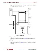
Communications between the KC724 board and a host computer are through a USB cable
connected to J79. Control is provided by U34, a USB-to-UART bridge (Silicon Laboratories
CP2103).
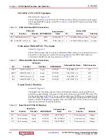
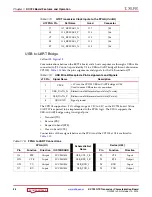
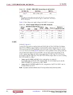
lists the pin assignments and signals for the USB connector J79.
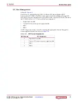
The CP2103 supports an I/O voltage range of 1.8V to 3.3V on the KC724 board. Xilinx
UART IP is expected to be implemented in the FPGA logic. The FPGA supports the
USB-to-UART bridge using four signal pins:
•
Transmit (TX)
•
Receive (RX)
•
Request to Send (RTS)
•
Clear to Send (CTS)
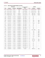
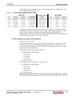
Connections of these signals between the FPGA and the CP2103 at U34 are listed in
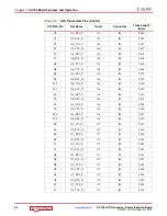
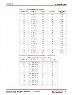
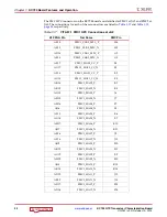
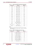
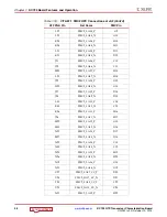
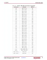
J7
117_REFCLK1_N
117
J85
C8
118_REFCLK0_P
118
J86
C7
118_REFCLK0_N
118
J86
E8
118_REFCLK1_P
118
J86
E7
118_REFCLK1_N
118
J86
Table 1-13:
GTX Transceiver Clock Inputs to the FPGA
(Cont’d)
U1 FPGA Pin
Net Name
Quad
Connector
Table 1-14:
USB Mini-B Receptacle Pin Assignments and Signals
J79 Pin
Signal Name
Description
1
VBUS
+5V into the CP2103 USB-to-UART bridge at U34.
Used to sense USB network connection.
2
USB_DATA_N
Bidirectional differential serial data (N-side).
3
USB_DATA_P
Bidirectional differential serial data (P-side).
4
GROUND
Signal ground.
Table 1-15:
FPGA to UART Connections
FPGA (U1)
Schematic Net
Name
Device (U34)
Pin
Function
Direction
IOSTANDARD
Pin
Function
Direction
J18
RTS
Output
LVCMOS18
USB_CTS_I_B
22
CTS
Input
H20
CTS
Input
LVCMOS18
USB_RTS_0_B
23
RTS
Output
G20
TX
Output
LVCMOS18
USB_RXD_I
24
RXD
Input
J17
RX
Input
LVCMOS18
USB_TXD_0
25
TXD
Output

