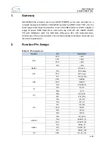
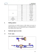
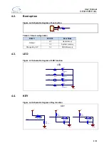
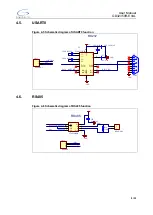
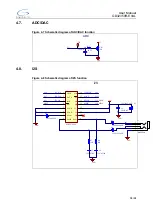
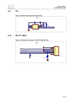
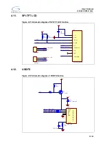
background image


GigaDevice Semiconductor Inc. 


GD32350R-EVAL 

User Manual 


Summary of Contents for GD32350R-EVAL

Page 1: ...GigaDevice Semiconductor Inc GD32350R EVAL User Manual ...

Page 2: ...ign 6 3 Getting started 7 4 Hardware layout overview 7 4 1 Power supply 7 4 2 Boot option 8 4 3 LED 8 4 4 KEY 8 4 5 USART0 9 4 6 RS485 9 4 7 ADC DAC 10 4 8 I2S 10 4 9 I2C 11 4 10 SPI TF CARD 11 4 11 SPI TFT LCD 12 4 12 USBFS 12 4 13 CMP 13 4 14 HDMI CEC 13 4 15 TSI 13 4 16 IFRP 14 4 17 RTC 14 4 18 GD Link 15 4 19 Extension 16 4 20 MCU 17 ...

Page 3: ...O Running Result 19 5 6 USART_DMA 20 5 6 1 DEMO Purpose 20 5 6 2 DEMO Running Result 20 5 7 RS485_Test 20 5 7 1 DEMO Purpose 20 5 7 2 DEMO Running Result 21 5 8 ADC_Conversion_Triggered_By_Timer 21 5 8 1 DEMO Purpose 21 5 8 2 DEMO Running Result 22 5 9 DAC_Output_Voltage_Value 22 5 9 1 DEMO Purpose 22 5 9 2 DEMO Running Result 22 5 10 Comparator_Obtain_Brightness 22 5 10 1 DEMO Purpose 22 5 10 2 D...

Page 4: ...MO Running Result 28 5 18 PMU_sleep_wakeup 29 5 18 1 DEMO Purpose 29 5 18 2 DEMO Running Result 29 5 19 RTC_Calendar 29 5 19 1 DEMO Purpose 29 5 19 2 DEMO Running Result 29 5 20 IRInfrared_Transceiver 29 5 20 1 DEMO Purpose 29 5 20 2 DEMO Running Result 30 5 21 TIMER_Breath_LED 30 5 21 1 DEMO Purpose 30 5 21 2 DEMO Running Result 30 5 22 TSI_TouchKey_leds 30 5 22 1 DEMO Purpose 30 5 22 2 DEMO Runn...

Page 5: ...function 10 Figure 4 9 Schematic diagram of I2C function 11 Figure 4 10 Schematic diagram of SPI TF CARD function 11 Figure 4 11 Schematic diagram of SPI TFT LCD function 12 Figure 4 12 Schematic diagram of USBFS function 12 Figure 4 13 Schematic diagram of CMP function 13 Figure 4 14 Schematic diagram of HDMI CEC function 13 Figure 4 15 Schematic diagram of TSI function 13 Figure 4 16 Schematic d...

Page 6: ...User Manual GD32350R EVAL 5 33 List of Tables Table 2 1 Pin assignment 6 Table 4 1 Boot configuration 8 Table 6 1 Revision history 33 ...

Page 7: ... Receiver RTC SPI USB ADC DAC and Extension Pin are also included This document details its hardware schematic and the relevant applications 2 Function Pin Assign Table 2 1 Pin assignment Function Pin Description LED PC10 LED1 PC11 LED2 PC12 LED3 PD2 LED4 RESET K1 Reset KEY PA0 K2 Wakeup PC13 K4 Temper PF7 K3 User Key USB PA11 USBDM PA12 USBDP PA9 USB VBUS IR PC6 IR_RX PB9 IR_TX I2C PB6 I2C0_SCL P...

Page 8: ...ter to get power the hardware system power is 3 3V A mini USB cable and a J Link tool are necessary to down programs Select the correct boot mode and then power on the LED6 will turn on which indicates the power supply is ready 4 Hardware layout overview 4 1 Power supply Figure 4 1 Schematic diagram of power supply G 1 Vout 2 Vin 3 4 U4 AMS1117 3 3 E5 16V 10uF AVX E6 16V 10uF AVX GND C20 50V 0 1uF...

Page 9: ...ory 1 2 System memory Changed by ISP 1 2 SRAM memory 4 3 LED Figure 4 3 Schematic diagram of LED function PC10 PC11 PC12 PC2 LED1 LED0603 LED2 LED0603 LED3 LED0603 LED4 LED0603 LED GND R25 470Ω R26 470Ω R27 470Ω R28 470Ω 4 4 KEY Figure 4 4 Schematic diagram of Key function PA0 R29 10KΩ 3V3 GND PC13 R31 10KΩ 3V3 GND C19 50V 0 1uF PF7 R30 10KΩ 3V3 GND C18 50V 0 1uF KEY K2 K 1102B K3 K 1102B K4 K 110...

Page 10: ...C28 50V 0 1uF C27 50V 0 1uF C25 50V 0 1uF C24 50V 0 1uF GND 1 6 2 7 3 8 4 9 5 J2 COM GND RS232 RS232_TX RS232_RX PA9 RS232_RX RS232_TX PA10 1 2 3 JP13 HEADER 3 PA9 RS232_TX USB_VBUS 4 6 RS485 Figure 4 6 Schematic diagram of RS485 function RO 1 RE 2 DE 3 DI 4 GND 5 A 6 B 7 Vcc 8 U6 ST485ABDR R38 120R 1 2 JP9 HEADER 2 C29 50V 0 1uF 3V3 GND GND RS485_DIR RS485_RX RS485_TX PA2 PA3 1 2 3 JP12 HEADER 3 ...

Page 11: ...I2S function LRCK 1 DATA 2 BCK 3 PD 4 AGND 5 HGND 6 Vcom 7 HoutR 8 SCKI 16 HoutL 9 AIN 10 Vhp 11 VCC 12 MD 13 MC 14 MS 15 U2 PCM1770 PM NRST GND 3V3 E2 16V 10uF AVX 5 4 3 2 1 J1 HeadPhone E3 10V 220uF AVX E4 10V 220uF AVX R7 16R R8 16R C5 50V 0 22uF C6 50V 0 22uF GND C4 50V 0 1uF E1 16V 10uF AVX GND GND PA4 PA7 PA5 PA6 PA15 I2S I2S_WS I2S_DIN I2S_CK I2S_MCK MSEL MCLK MDIN I2S_MCLK I2S_MDIN ...

Page 12: ...4 SDA 5 SCL 6 WP 7 VCC 8 U1 AT24C02C SSHM T 3V3 GND R5 4 7KΩ R6 4 7KΩ C3 50V 0 1uF GND I2C 4 10 SPI TF CARD Figure 4 10 Schematic diagram of SPI TF CARD function 3V3 3V3 PB4 PF4 SD LCD_SPI_CLK SD LCD_SPI_MOSI D2 1 D3 2 CMD 3 VCC 4 CLK 5 GND 6 D0 7 D1 8 CD 9 CN2 TF_CARD_SOCKET GND GND E0 16V 10uF AVX SPI R41 10KΩ ...

Page 13: ... 3 JP10 HEADER 3 1 2 3 JP11 HEADER 3 PB3 PB5 SD LCD_SPI_CLK SD LCD_SPI_CLK SD LCD_SPI_MOSI SD LCD_SPI_MOSI I2S_MCLK I2S_MDIN C30 50V 0 1uF 3V3 3V3 R44 10KΩ 4 12 USBFS Figure 4 12 Schematic diagram of USBFS function GND R54 47KΩ R55 470R R33 22R R34 22R PD2 E10 16V 10uF AVX GND PA11 PA12 1 2 3 Q3 S8550 R37 1MΩ C22 50V 4700pF PWR USB_VBUS USB_DM USB_DP VBUS 1 DM 2 DP 3 ID 4 GND 5 Shield 6 USB_MiniAB...

Page 14: ...f CMP function R22 8 2K R23 VT9ON1 3V3 R21 0 CMP0 COMPARATOR 4 14 HDMI CEC Figure 4 14 Schematic diagram of HDMI CEC function R24 27KΩ 3V3 1 2 JP7 HEADER 2 GND PB8 HDMI CEC 4 15 TSI Figure 4 15 Schematic diagram of TSI function R24 27KΩ 3V3 1 2 JP7 HEADER 2 GND PB8 HDMI CEC ...

Page 15: ...atic diagram of IFRP function 3V3 1 2 3 Q2 8050 GND R10 1KΩ R9 100Ω PB9 LED5 KD 03144R 1 2 3 JP2 HS0038B 5V GND GND PC6 R11 10KΩ C2 10V 4 7uF R43 100Ω IFRP 4 17 RTC Figure 4 17 Schematic diagram of RTC function 1 2 3 JP5 Vbat select VBAT 1 2 BT1 Battety GND 3V3 ...

Page 16: ... NRST 7 OSC_IN PD0 5 OSC_OUT PD1 6 PA0 WKUP 10 PA1 11 PA2 12 PA3 13 PA4 14 PA5 15 PA6 16 PA7 17 PA8 29 PA9 30 PA10 31 PA11 32 PA12 33 PA13 JTMS SWDIO 34 PA14 JTCK SWCLK 37 PA15 JTDI 38 PB0 18 PB1 19 PB2 BOOT1 20 PB3 JTDO 39 PB4 JNTRST 40 PB5 41 PB6 42 PB7 43 PB8 45 PB9 46 PB10 21 PB11 22 PB12 25 PB13 26 PB14 27 PB15 28 PC13 TAMPER RTC 2 PC14 OSC32_IN 3 PC15 OSC32_OUT 4 VBAT 1 VDD_1 24 VDD_2 36 VDD...

Page 17: ... JP6 HEADER 16X2 1 2 3 4 5 6 7 8 9 10 11 12 13 14 15 16 17 18 19 20 21 22 23 24 25 26 27 28 29 30 31 32 JP8 HEADER 16X2 PA14 PA15 PC10 PC11 PC12 PD2 PB3 PB4 PB5 PB6 PB7 BOOT0 PB8 PB9 GND PC13 PC14 PC15 PC0 PC1 PC2 PC3 PA0 PA1 PA2 PF7 PF6 PA13 PA12 PA11 PA10 PA9 PA8 PC9 PC8 PC7 PC6 PB15 PB14 PB13 PB12 GND PB11 PB10 PB2 PB1 PB0 PC5 PC4 PA7 PA6 PA5 PA4 PF5 PF4 PA3 3V3 3V3 EXTENTION ...

Page 18: ...C12 53 PC13 2 PC14 OSC32_IN 3 PC15 OSC32_OUT 4 PD2 54 VBAT 1 VDD_2 32 PF7 48 VDD_1 64 PF5 19 VDDA VREF 13 VSS_2 31 PF6 47 VSS_1 63 PF4 18 VSSA VREF 12 U3 GD32F350RxT6 PA0 PA1 PA2 PA7 PA6 PA5 PA4 PA13 PA12 PA11 PA10 PA9 PA8 PA14 PA15 PB2 PB1 PB0 PB6 PB7 PB3 PB4 PB5 PC1 PC0 PC2 PC3 PC9 PC8 PC7 PC6 5 Routine use guide 5 1 GPIO_Runing_Led 5 1 1 DEMO Purpose This Demo includes the following functions o...

Page 19: ...wnload the program 02_GPIO_KeyBoard_Polling_mode to the EVAL board first of all all the LEDs will be flashed once for test Then press down the Tamper Key LED2 will be turned on Press down the Tamper Key again LED2 will be turned off 5 3 GPIO_KeyBoard_Interrupt_mode 5 3 1 DEMO Purpose This Demo includes the following functions of GD32 MCU Learn to use GPIO to control the LED and the KEY Learn to us...

Page 20: ...pt 5 5 1 DEMO Purpose This Demo includes the following functions of GD32 MCU Learn to use the EVAL_COM transmit and receive interrupts to communicate with the hyperterminal 5 5 2 DEMO Running Result Jump JP13 to USART then download the program 05_USART_HyperTerminal_ Interrupt to the EVAL board and run Firstly all the LEDs are turned on and off for test Then the COM sends the tx_buffer array from ...

Page 21: ...e hyperterminal and waits for receiving data from the hyperterminal that you must send The string that you have sent is stored in the rx_buffer array The receive buffer have a BUFFER_SIZE bytes as maximum After that compare tx_buffer with rx_buffer If tx_buffer is same with rx_buffer LED1 and LED2 are turned on LED3 and LED4 are turned off Otherwise LED1 and LED2 are turned off LED3 and LED4 are t...

Page 22: ...itter and LED2 is on and when press the Tamper key on one board the board is set as RS485 receiver and LED3 is on Download the program 07_RS485_Test to the EVAL board and run the information via a serial port output as following According to the tips press down Wakeup key to set one board as a transmitter and press down Tamper key to the other as a receiver The transmitter output as following The ...

Page 23: ...s of GD32 MCU Learn to use DAC channel to generate different voltages on DAC output 5 9 2 DEMO Running Result Download the program 09_DAC_Output_Voltage_Value to the EVAL board the digital value is 0x7ff0 its converted analog voltage should be VREF 2 using the voltmeter to measure PA4 its value is 1 648V 5 10 Comparator_Obtain_Brightness 5 10 1 DEMO Purpose This Demo includes the following functio...

Page 24: ...ble to COM and open the HyperTerminal to show the print message Firstly the data of 256 bytes will be written to the EEPROM from the address 0x00 and printed by the serial port Then reading the EEPROM from address 0x00 for 256 bytes and the result will be printed Finally compare the data that were written to the EEPROM and the data that were read from the EEPROM If they are the same the serial por...

Page 25: ...read data from the original address check the correctness of the written and read data Note that the FATFS is not used in this demo and in the absence of FATFS read and write to the TF card will destroy the file system please make a backup before testing 5 12 2 DEMO Running Result Firstly JP10 and JP11 must be fitted to SPI and then download the program 12_SPI_TF_Card_Block_Operation to the EVAL b...

Page 26: ...mation will be displayed on the LCD screen 5 13 2 DEMO Running Result Firstly JP10 and JP11 must be fitted to SPI and then download the program 13_SPI_TF_Card_FATFS_Operation to the EVAL board All the LEDs are turned on and then turned off for test Insert a formatted TF card a text file will be created in this TF card When the screen appears FATFS FILE Create Success you can remove the TF card and...

Page 27: ...LCD screen which supports SPI interface In this demo tests of font number draw and color are displayed on the LCD screen respectively 5 14 2 DEMO Running Result Firstly JP10 and JP11 must be fitted to SPI port and then download the program 14_SPI_TFT_LCD_Driver to the EVAL board All the LEDs are turned on and then turned off for test After that the LCD screen on the board will display the GUI test...

Page 28: ...d one board as a sender the other as a receiver First use the DuPont to connect CEC bus PB8 and ground wire GND pins in the two board and then download the program 15_HDMI_CEC_HostSlaveCommunication to the board for running When the program runs the first development board of the LCD display is data 0 press one of the development board TAMPER key the other piece of the development board LCD number...

Page 29: ... file 5 17 RCU_Clock_Out 5 17 1 DEMO Purpose This Demo includes the following functions of GD32 MCU Learn to use GPIO control the LED Learn to use the clock output function of RCU Learn to communicate with PC by USART 5 17 2 DEMO Running Result Download the program 17_RCU_Clock_Out to the EVAL board and run Connect serial cable to EVAL_COM open the HyperTerminal When the program is running HyperTe...

Page 30: ...C module to implement calendar function Learn to use LCD module to display the time of calendar 5 19 2 DEMO Running Result Download the program 19_RTC_Calendar to the EVAL board and run When the program is running the four LEDs LED1 to LED4 turn on then turn off And then the LCD prints out the information of the board and the calendar When you press the Wakeup key the time will be configured to 20...

Page 31: ...d LED1 PC10 and then download the program 21_TIMER_Breath_LED to the GD32350R EVAL board and run PA8 should not be reused by other peripherals When the program is running you can see LED1 lighting from dark to bright gradually and then gradually darken ad infinitum just like breathing as rhythm 5 22 TSI_TouchKey_leds 5 22 1 DEMO Purpose This Demo includes the following functions of GD32 MCU Learn ...

Page 32: ...sult Download the program 23_USB_Device CDC_ACM to the EVAL board and run When you input message through computer keyboard the HyperTerminal will receive and shown the message For example when you input GigaDevice MCU the HyperTerminal will get and show it as below 5 23 2 USBD_Keyboard DEMO Purpose This demo includes the following functions of GD32 MCU Learn how to use the USBFS peripheral mode Le...

Page 33: ...eup function you can do as follows Manually switch PC to standby mode Wait for PC to fully enter the standby mode Push the Wakeup key If PC is ON remote wakeup is OK else failed 5 24 USB_Host 5 24 1 USBH_HID_Host DEMO Purpose This demo includes the following functions of GD32 MCU Learn to use the USBFS as a HID host Learn the operation between the HID host and the mouse device Learn the operation ...

Page 34: ...the operation between the MSC host and the Udisk EVAL evaluation board integrates the USBFS module and the module can be used as USBFS device a USBFS host or OTG device This demo mainly shows how to use the USBFS as a USB MSC host to communicate with external Udisk DEMO Running Result Jump the JP13 to USB Then insert the OTG cable to the USB port download the program 24_USB_Host USBH_MSC to the EV...

Page 35: ...RENCE BOARD MPC574XG MB BSC9132QDS C29XPCIE RDB KIT_TC1793_SK CC ACC 18M433 P1010RDB PB P1020RDB PD P2020COME DS PB STM8S 32 D RAIS T4240RDB PB TRK USB MPC5604B TWR 56F8200 CY3674 SPC58XXADPT176S MAX1464EVKIT TRK MPC5606B RTE510Y470TGB00000R STM8128 MCKIT MAXQ622 KIT YRPBRL78G11 SPC58EEMU QB R5F10JGC TB YQB R5F11BLE TB SPC564A70AVB176 RTE5117GC0TGB00000R QB R5F100LE TB YR0K50571MS000BE YQB R5F1057...

Reviews: