
Design Guide
SiRF Proprietary and Confidential
SiRFatlasV
Hardware Design Guide
January 2010
Document Number: CS-129512-UG
Issue 3
I
NTRODUCTION
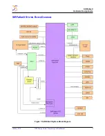
This document serves as a hardware design guide for the
SiRFatlasV™ SoC based Evaluation Board
(EVB) including boot configuration, power supply, and peripheral interfaces such as RAM, ROM, USB
and more. For details about the schematics, contact SiRF field application engineers (FAE).