Manual PCI-A12-16A
16
Register Descriptions
Offset 0 Write
Start Conversion
This address is written to if you wish to start a conversion programmatically. Any value written to this address
will cause the A/D to perform a conversion on the currently selected channel at the currently selected range.
Use the A/D Control register at Offset 2 to select the channel and range. Conversions may also be started via
an External Start Conversion signal (pin 4, see Offset 4) or via Counters (see Offset 4).
Offset 1 Write
Unused
This address is unused, writes are ignored.
Offset 0 Read
A/D Data (Low byte)
Offset 1 Read
A/D Data (High SEL readback)
These addresses allow you to read the data stored in the data FIFO. The data is read oldest to newest. The
values of SEL3-0 are placed in the four most significant bits of Offset 1 and may be used as a data tag.
Since the data is contained in both of these registers, it is a good practice to read Offset 0 and Offset 1 with a
single word read command to assure that the two data registers stay properly synchronized.
Data is presented in two's complement form. The following shows the bit positions of the data returned:
Read as 16-bit integer from Offset 0
Read as byte from Offset 1
Read as byte from Offset 0
sel3 sel2 sel1 sel0 DB DA D9 D8 D7 D6 D5
D4 D3 D2 D1 D0
Read a single 16-bit integer and mask off the high-order 4 bits to obtain a value. See the programming guide
at the end of this chapter for more information.
Sel3 through Sel0 are a readback of the state of the Sel3 through Sel0 bits associated with the point in the
point list FIFO that started the conversion. See Offset 2&3 for an explanation of the Sel bits.
Offset 2&3 Write
A/D Control
Setup Point List
Offset 2&3 Read
A/D Control
Readback
This address (base+2) should be written to using a 16-bit WORD command (out dx,ax). Doing so loads the
point-list FIFO. Repeated writes to this address are used to load an entire point-list into the FIFO for later use.
The format of the WORD is described below. After loading up to 4096 WORDS, you must read a WORD from
this address before starting conversions. Refer to the programming guide at the end of this chapter for more
information on using this register.
Note: it is very useful to use SEL3-SEL0 as markers, as long as external muxes are not being used, to track
which channel data is from. When no external mux is being used, writing the same value to SEL3-SEL0 as
MA3-MA0 causes the data FIFO to appear to hold the channel number (MA3-0), which enables easier
tracking of data and channel number.
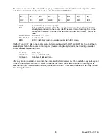
The following diagrams define bit functions in the point list:
bit 7
bit 6
bit 5
bit 4
bit 3
bit 2
bit 1
bit 0
MA3 MA2 MA1 MA0 DIFF R2 R1 R0
bit 15
bit 14
bit 13
bit 12
bit 11
bit 10
bit 9
bit 8
SEL3 SEL2 SEL1 SEL0 (unused)
G2
G1
G0


