background image

Manual PCI-A12-16A 

19

Offset 10, 11, and 12  8255 Digital I/O Ports


These registers are the ports of the 8255; offset 10 is port A, offset 11 is port B, and offset 12 is port C. Each 
port is 8 bits, for a total of 24 bits. Each port’s direction can configured independently via the control register 
at offset 13. All ports power up as input ports. Each bit has a weak pull-up, so that with no signal applied, all 
inputs read high. 
  
Writing to an output port will update the data on that port. Reading from an output port will read back the 
output data. Reading from an input port will read the current data on that port. Writing to an input port is 
ignored. 
  
Port C can be treated as two 4-bit ports, C Hi (bits 4-7) and C Lo (bits 0-3), instead of a single 8-bit port. 
Often, one is configured as an input port and the other as an output port, to provide a few control signals in 
each direction. Since writes to inputs are ignored, one can be written to without affecting the inputs of the 
other. 
  

Offset 13 


8255 Control


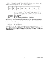
This register is normally used to control the direction of the 8255 digital I/O ports. Port modes can also be set 
here, however the card is only designed for mode 0; contact the factory for a custom solution if modes 1 or 2 
are desired. Bit assignments in this control byte are as follows: 
 

Bit


Assignment


Function


D0 

Port C Lo (C0-C3) 

1 = Input, 0 = Output 

D1 

Port B 

1 = Input, 0 = Output 

D2 

Mode Selection (B & C Lo) 

Use 0 

D3 

Port C Hi (C4-C7) 

1 = Input, 0 = Output 

D4 

Port A 

1 = Input, 0 = Output 

D5 

Mode Selection (A & C Hi) 

Use 0 

D6 

Mode Selection (Mode 2) 

Use 0 

D7 

Mode Set Flag 

Use 1 

  
Three common control bytes (in hex): 
 

80 - Set all ports to output. 


9B - Set all ports to input. This is their power-on configuration. 


83 - Set ports A and C Hi to output, set ports B and C Lo to input. 


Summary of Contents for PCI-A12-16A

Page 1: ...ess underutilized and idle equipment along with credit for buybacks and trade ins Custom engineering so your equipment works exactly as you specify Critical and expedited services Leasing Rentals Demos In stock Ready to ship TAR certified secure asset solutions Expert team I Trust guarantee I 100 satisfaction All trademarks brand names and brands appearing herein are the property of their respecti...

Page 2: ...10623 Roselle Street San Diego CA 92121 858 550 9559 FAX 858 550 7322 contactus accesio com www accesio com MODEL PCI A12 16A USER MANUAL FILE MPCI A12 16A A1o ...

Page 3: ...S nor the rights of others IBM PC PC XT and PC AT are registered trademarks of the International Business Machines Corporation Printed in USA Copyright 2004 2006 by ACCES I O Products Inc 10623 Roselle Street San Diego CA 92121 All rights reserved WARNING ALWAYS CONNECT AND DISCONNECT YOUR FIELD CABLING WITH THE COMPUTER POWER OFF ALWAYS TURN COMPUTER POWER OFF BEFORE INSTALLING A CARD CONNECTING ...

Page 4: ...r parts not excluded by warranty Warranty commences with equipment shipment Following Years Throughout your equipment s lifetime ACCES stands ready to provide on site or in plant service at reasonable rates similar to those of other manufacturers in the industry Equipment Not Manufactured by ACCES Equipment provided but not manufactured by ACCES is warranted and will be repaired according to the t...

Page 5: ...Installation 10 WINDOWS 10 LINUX 10 Hardware Installation 11 Chapter 3 Option Selection 12 Figure 3 1 Option Selection Map 13 Chapter 4 Address Selection 14 Chapter 5 Programming 15 Table 5 1 Register addresses on the card hex 15 Register Descriptions 16 Software Tristate Mode 20 Programming Guide 21 Chapter 6 Programmable Interval Timer 24 Operational Modes 24 Programming 26 Programming Examples ...

Page 6: ...little processor overhead A D conversions may be initiated in any of three ways a software command b an on board programmable timer or c direct external trigger In turn data may be transferred to the computer by any of three software selectable methods a polling for end of conversion EOC b polling for a half full FIFO or c a half FIFO interrupt Input System Expansion This card can be used with up ...

Page 7: ...y an AD7237 dual DAC They are independently configurable by means of on board switches Each may be configured to unipolar or bipolar outputs and may have full scale ranges of 2 5 5 or 10 volts Interrupts This card has interrupt capability within the PCI bus The interrupt for the card can be software enabled and can be initiated by various FIFO status conditions Transferring Data into the Computer ...

Page 8: ...Software selectable external trigger programmable timer or program command Sample and Hold Amplifier Acquisition Time 1 microsecond to 0 01 typical for full scale step function input Aperture Uncertainty 0 3 nanosecond typical Reference Voltage Output Voltage 10VDC 0 25VDC Temp Coefficient 30 ppm C Load Drive 200mA maximum Digital I O Inputs Logic high 2 0 to 5 0 VDC at 20 uA maximum at 2 7V Logic...

Page 9: ... down counters two permanently concatenated with 1MHz clock as programmable timer Output Drive 2 2mA at 0 45V 5 LSTTL loads Input Gate TTL DTL CMOS compatible Clock Frequency DC to 10MHz Active Count Edge Negative edge Min Clock Pulse Width 30nS high 50nS low Timer Range 2 5 MHz to 1 pulse hr Environmental Operating Temp 0 C to 50 C Storage Temp 20 C to 70 C Humidity 0 to 90 RH non condensing Powe...

Page 10: ...S DECODE SELECT CONTROL REGISTER INTERRUPT CONTROL TRIGGER SELECT LOGIC DAC 0 AND DAC 1 7 BIT OUTPUT REGISTER SUBMUX CONTROL 1 2 4 8 GAIN SELECT INTERNAL DATA BUS I B M P C I B U S A D TRIG DAC 0 GN0 GN1 GN2 SEL0 SEL1 SEL2 SEL3 DAC 1 CH0 HI CH0 LO CH15 16 BIT CTR 0 16 BIT CTR 1 16 BIT CTR 2 1MHz XTAL CTR0 CLOCK IN CTR2 OUT I I I G G G O O O 8255 DIGITAL INPUT OUTPUT INTERFACE 24 BITS TTL DIGITAL I...

Page 11: ...ion with Chapter 3 to assist in configuring jumpers on the card as well as provide additional descriptions for usage of the various card options CD Software Installation The following instructions assume the CD ROM drive is drive D Please substitute the appropriate drive letter for your system as necessary WINDOWS 1 Place the CD into your CD ROM drive 2 The system should automatically run the inst...

Page 12: ...nding on the operating system and automatically finish installing the drivers 9 Run PCIfind exe to complete installing the card into the registry for Windows only and to determine the assigned resources 10 Run one of the provided sample programs that was copied to the newly created card directory from the CD to test and validate your installation The base address assigned by BIOS or the operating ...

Page 13: ...fer Enable Buffer Tristate BEN BTR jumper enables or disables software tristating of the digital I O bits Normally this jumper will be installed in the BEN position In order to use the software tristate feature install this jumper in the BTR position this will change the behavior of the DIO bits as described in the Programming chapter The range of each DAC is set by a block of switches on the boar...

Page 14: ...Manual PCI A12 16A 13 RP1 RP2 RP3 CH0 CH7 FACTORY USE ONLY SELECT INPUT CHANNEL AS 4 20mA RP5 RP6 RP7 RP8 BTR BEN DAC0 DAC1 Pin 1 Figure 3 1 Option Selection Map ...

Page 15: ...operating systems you can use either PCIFind or the Device Manager utility from the System Properties Applet of the control panel The card is installed in the Data Acquisition class of the Device Manager list Selecting the card clicking Properties and then selecting the Resources Tab will display a list of the resources allocated to the card The PCI bus supports 64K of I O address space so your ca...

Page 16: ... unused unused 6 unused unused 7 unused unused 8 8254 Counter Timer 0 8254 Counter Timer 0 9 8254 Counter Timer 1 8254 Counter Timer 1 A 8254 Counter Timer 2 8254 Counter Timer 2 B 8254 Counter Timer Control 8254 Counter Timer Status C DAC 0 8 LSB unused D DAC 0 4 MSB unused E DAC 1 8 LSB unused F DAC 1 4 MSB unused 10 8255 Port A Output 8255 Port A Input Readback 11 8255 Port B Output 8255 Port B...

Page 17: ... D5 D4 D3 D2 D1 D0 Read a single 16 bit integer and mask off the high order 4 bits to obtain a value See the programming guide at the end of this chapter for more information Sel3 through Sel0 are a readback of the state of the Sel3 through Sel0 bits associated with the point in the point list FIFO that started the conversion See Offset 2 3 for an explanation of the Sel bits Offset 2 3 Write A D C...

Page 18: ...polar 5 volts 5 volt span 0 to 5V 1 1 0 6 unipolar 1 25 to 3 75 volts 2 5 volt span 1 1 1 7 unipolar 1 25 to 6 25 volts 5 volt span The 1 25 6 25 volt range is designed for use with the Current Mode jumper on each channel Selecting this range for those channels that have been placed in current mode results in a 4 20mA range with full 12 bit precision SEL3 SEL2 SEL1 SEL0 G2 G1 G0 These bits are dig...

Page 19: ...e status of various features on the card primarily the state of the point list and data FIFOs or to determine if a conversion has finished bit 7 bit 6 bit 5 bit 4 bit 3 bit 2 bit 1 bit 0 BUSY CFF CFH CF0 FF FH F0 EXT The BUSY bit indicates the conversion is in process A zero means the A D is busy a one means a conversion is not in progress This bit is one of the most important when not using inter...

Page 20: ...red as an input port and the other as an output port to provide a few control signals in each direction Since writes to inputs are ignored one can be written to without affecting the inputs of the other Offset 13 8255 Control This register is normally used to control the direction of the 8255 digital I O ports Port modes can also be set here however the card is only designed for mode 0 contact the...

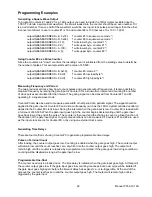
Page 21: ...se which would trigger latched sensors To alleviate this issue this card has a software tristate mode enabled by installing the BEN BTR jumper in the BTR position In software tristate mode whenever a control byte is written all ports are tristated Your software should re initialize the output ports then de tristate them causing them to all update simultaneously Pull ups on the card cause tristated...

Page 22: ...ta from a single range and usually at a single SE DIFF setting These two values then can be hard coded into the program and the code becomes control CH 4 1 for Single ended 5 VDC operation Write two or more of these points to the point list and that is all there is for polled mode A D conversions The data comes back in counts and must be converted to engineering units to be useful The data is retu...

Page 23: ... Enable Counter Mode Offset 4 Write loop Wait for FIFO Half full Offset 4 Read Read Data until FIFO empty Offset 0 Read 16 bit integer Offset 4 Read Loop at loop until you have as much data as you want This mode can be used to easily test point list setup and general FIFO functionality but generally won t be used in real world environments IRQ based FIFO handling is so efficient that most applicat...

Page 24: ...he IRQ vector table Once these are grasped however the benefits are well worth the learning curve IRQ mode is a great way to perform non data gathering tasks while conversions are taking place The background task the ISR takes data and stores it while the foreground task can perform other functions such as display calculations or acquisition from some other device This mode is so useful that an ex...

Page 25: ...nter Loading Programming of a binary count into the counter Mode 0 Pulse on Terminal Count After the counter is loaded the output is set low and will remain low until the counter decrements to zero The output then goes high and remains high until a new count is loaded into the counter A trigger enables the counter to start decrementing This mode is commonly used for event counting with Counter 0 M...

Page 26: ...repeat the cycle A low gate input will inhibit the counter This mode can be used to provide a delayed software trigger for initiating A D conversions Mode 5 Hardware Triggered Strobe In this mode the counter will start counting after the rising edge of the trigger input and will go low for one clock period when the terminal count is reached The counter is retriggerable The output will not go low u...

Page 27: ...ter mode the type of read write operation and the modulus The control byte format is as follows Base B Write Counter Control Byte B7 B6 B5 B4 B3 B2 B1 B0 SC1 SC0 RW1 RW0 M2 M1 M0 BCD SC0 SC1 These bits select the counter that the control byte is destined for SC1 SC0 Function 0 0 Program Counter 0 0 1 Program Counter 1 1 0 Program Counter 2 1 1 Read Write Cmd See section on Reading and Loading the ...

Page 28: ...ed counter returns the held value Latching is the best way to read a counter on the fly without disturbing the counting process You can only rely on directly read counter data if the counting process is suspended while reading by bringing the gate low or by halting the input pulses For each counter you must specify in advance the type of read or write operation that you intend to perform You have ...

Page 29: ...command M2 M1 M0 Counter mode BCD BCD 0 is binary mode otherwise counter is in BCD mode If both STA and CNT bits in the counter status byte are set low and the RW1 and RW0 bits have both been previously set high in the counter control register thus selecting two byte reads then reading a selected counter address location will yield 1st Read Status byte 2nd Read Low byte of latched data 3rd Read Hi...

Page 30: ...n a square wave mode Counter 0 can also be used to measure pulse width or half period of a periodic signal The signal should be applied to the gate input of Counter 0 and a known frequency such as the 1MHz crystal controlled oscillator applied to the Counter 0 clock input During the interval when the gate input is low Counter 0 is loaded with a full count of 65 535 When the gate input goes high th...

Page 31: ...ed a programmed duration after the counter is loaded Hardware Triggered Strobe This is similar to Programmable One Shot except that when the counter is triggered by the gate going high the counter output immediately goes high then goes low for one clock period at timeout producing a negative going strobe pulse The timeout is re triggerable i e a new cycle will commence if the gate goes high before...

Page 32: ... The cards are calibrated through a software routine contained in the setup program Once the card is setup run the calibration sequence as shown in the program and make the calibration adjustments on RP1 RP2 RP3 RP5 RP6 RP7 and RP8 on the board ...

Page 33: ... Output 1 16 no connection 17 IN8 Chl 7 Analog Low Input Diff l Chl 15 Analog High Input SE 18 AGround Low Level Analog Common Ground 19 VREF 10VDC Reference Voltage 20 VSS 12VDC 21 IN7 Chl 6 Analog Low Input Diff l Chl 14 Analog High Input SE 22 IN6 Chl 5 Analog Low Input Diff l Chl 13 Analog High Input SE 23 IN5 Chl 4 Analog Low Input Diff l Chl 12 Analog High Input SE 24 IN4 Chl 3 Analog Low In...

Page 34: ...ort C Hi Bit 5 5 6 Port C Hi Bit 4 7 8 Port C Lo Bit 3 9 10 Port C Lo Bit 2 11 12 Port C Lo Bit 1 13 14 Port C Lo Bit 0 15 16 Port B Bit 7 17 18 Port B Bit 6 19 20 Port B Bit 5 21 22 Port B Bit 4 23 24 Port B Bit 3 25 26 Port B Bit 2 27 28 Port B Bit 1 29 30 Port B Bit 0 31 32 Port A Bit 7 33 34 Port A Bit 6 35 36 Port A Bit 5 37 38 Port A Bit 4 39 40 Port A Bit 3 41 42 Port A Bit 2 43 44 Port A B...

Page 35: ...manual or just want to give us some feedback please email us at manuals accesio com Please detail any errors you find and include your mailing address so that we can send you any manual updates 10623 Roselle Street San Diego CA 92121 Tel 858 550 9559 FAX 858 550 7322 www accesio com ...

Page 36: ...quipment Have surplus equipment taking up shelf space We ll give it a new home Learn more Visit us at artisantg com for more info on price quotes drivers technical specifications manuals and documentation Artisan Scientific Corporation dba Artisan Technology Group is not an affiliate representative or authorized distributor for any manufacturer listed herein We re here to make your life easier How...

Reviews: