T5L_ASIC Development Guide
- 31
-
www.dwin-global.com
DWIN Technology
Professional,
Creditable,
S
uccessful
3.8 CAN
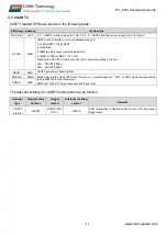
The SFRs associated with the CAN interface are shown in the following table :
SFR name Address
Instructions
MUX_SEL
0xC9
.7 1 = CAN interface leads to P 0.4 and P 0.5,0 = CAN interface does not lead out, it is IO port .
CAN_CR
0x8F
CAN interface control register
.7 CAN interface enable.1=open; 0=close;
.6 CAN interface mode. 1=software reset; 0=working normally;
.5 Write 1 to configure data of CAN interface once (0xFF:0060-0xFF:0062), and clear after hardware
processing;
.4 Set speed mode. 1 = 1 sampling;
0 = 3 sampling;
.3 Setting filter mode.1=double; 0=single;
.2 Write 1 to send once, and clear after hardware processing (sending success, arbitration failure, EI
(CAN_IR.3) occurred, software reset);
.1-0 Undefined, write 0.
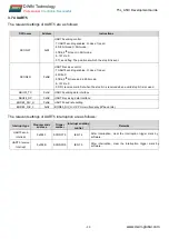
CAN_IR
0x91
CAN interface interrupt status register
.7 RF_IF. Remote frame receiving interrupt mark, and clear after hardware placement;
.6 CAN_RX_IF. CAN receiving interrupt mark, and clear after hardware placement. During the placement,
the hardware can no longer update the data;
.5 CAN_RX_IF, CAN sending interrupt mark, and clear after hardware placement;
.4 OI, receiving overflow markers, hardware blanking, software clearance is required;
.3 EI, error mark. CAN_ET[4:0] has an error generated when this bit is pulled high and needs to be
cleared by software
.2 JI, send arbitration mark. 1 = send arbitration failure; 0 = send arbitration success;
.1-.0 Undefined.
CAN_ET
0xE8
CAN interface error type register and clear after hardware placement. Addressable by bit.
.7 Node suspension identification;
.6 Active error identification;
.5 Passive error identification;
.4 CRC check error identification;
.3 Response error identification;
.2 Format error identification;
.1 Bit filling error identification;
.0 Bit error identification.
The CAN communication interface is defined in terms of DGUS variable space. The related variables
are as below.
Address Position Length Definition
Instructions
0xFF:0060
D3
1
BRP
BRP: Baud rate frequency divider register
BTR0: [7:5] is the synchronous jump width sjw, [3:0] prop propagation time T0.
BTR1: [7:4] is phase buffer segment 1, T1, [3:0] is phase buffer segment 2, T2.
T0+T1+T2=CPU main frequency/(baud rate*(BRP*2+1))-4
D2
1
BTR0
D1
1
BTR1
D0
1
Undefined,
write 0
0xFF:0061 D3:D0
4
ACR3:0
Acceptance code register


