Rev. 1.60
146
August 20, 2019
Rev. 1.60
147
August 20, 2019
BS66F340/BS66F350/BS66F360/BS66F370
Touch A/D Flash MCU with LED Driver
BS66F340/BS66F350/BS66F360/BS66F370
Touch A/D Flash MCU with LED Driver
Registers Descriptions
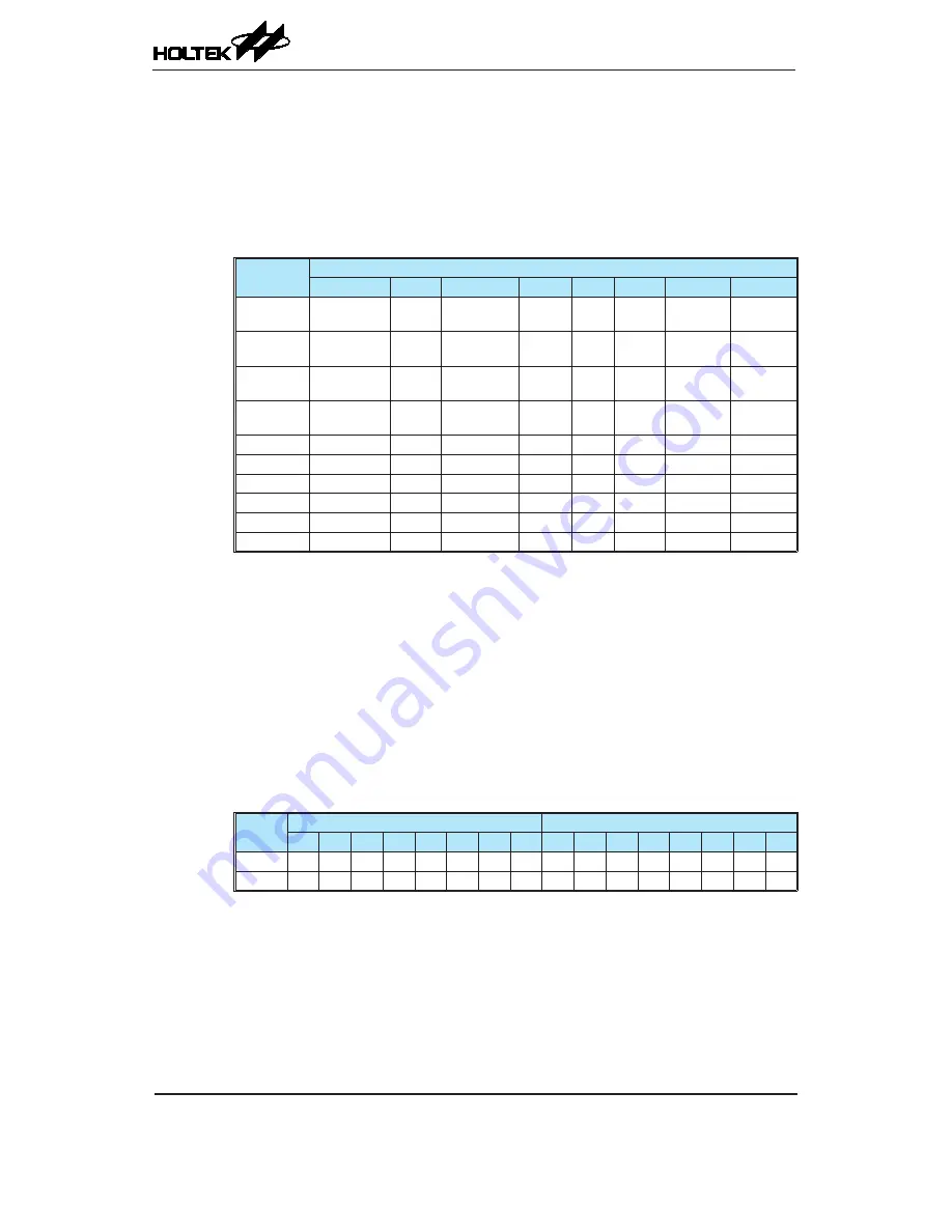
Overall operation of the A/D converter with Temperature sensor is controlled using eight registers.
A read only register pair exists to store the A/D Converter data 12-bit value. Two registers, ADCR0
and ADCR1, are the control registers which setup the operating and control function of the A/D
converter. The remaining four registers are the temperature sensor control registers which select
the temperature sensor signal to be converted and the reference voltage source together with the
temperature sensor conversion clock cycles.
Register
Name
Bit
7
6
5
4
3
2
1
0
ADRL
(ADRFS=0)
D3
D2
D1
D0
—
—
—
—
ADRL
(ADRFS=1)
D7
D6
D5
D4
D3
D2
D1
D0
ADRH
(ADRFS=0)
D11
D10
D9
D8
D7
D6
D5
D4
ADRH
(ADRFS=1)
—
—
—
—
D11
D10
D9
D8
ADCR0
START
ADBZ
ADCEN
ADRFS ACS3 ACS2
ACS1
ACS0
ADCR1
ATM
—
IDLE_CONV VREFS
—
ADCK2
ADCK1
ADCK0
TSC0
BGMEN
G5XEN
K_REFO
—
—
—
—
—
TSC1
TSE
OP2EN
OP1EN
—
—
—
—
—
TSC2
VREFP_EXT BIAS
D5
D4
D3
D2
TSCLK_S1 TSCLK_S0
TSC3
—
—
K_VPTAT
—
—
—
—
—
A/D Converter with Temperature Sensor Registers List
A/D Converter Data Registers – ADRL, ADRH
As these devices contain an internal 12-bit A/D converter, it requires two data registers to store the
converted value. These are a high byte register, known as ADRH, and a low byte register, known
as ADRL. After the conversion process takes place, these registers can be directly read by the
microcontroller to obtain the digitised conversion value. As only 12 bits of the 16-bit register space
is utilised, the format in which the data is stored is controlled by the ADRFS bit in the ADCR0
register as shown in the accompanying table. D0~D11 are the A/D conversion result data bits. Any
unused bits will be read as zero. Note that the A/D data register contents can only be read in the A/
D conversion completion interrupt service subroutine when the Auto-conversion mode is enabled by
setting the ATM bit in the ADCR1 register to 1. The A/D data registers contents will be cleared to
zero if the A/D converter is disabled.
ADRFS
ADRH
ADRL
7
6
5
4
3
2
1
0
7
6
5
4
3
2
1
0
0
D11 D10 D9 D8 D7 D6 D5 D4 D3 D2 D1 D0
0
0
0
0
1
0
0
0
0
D11 D10 D9 D8 D7 D6 D5 D4 D3 D2 D1 D0
A/D Converter Data Registers
A/D Converter Control Registers – ADCR0, ADCR1
To control the function and operation of the A/D converter, two control registers known as ADCR0
and ADCR1 are provided. These 8-bit registers define functions such as the selection of which
analog channel is connected to the internal A/D converter, the digitised data format, the A/D clock
source as well as controlling the start function and monitoring the A/D converter busy status. As
these devices contain only one actual analog to digital converter hardware circuit, each of the
external and internal analog signals must be routed to the converter. The ACS3~ACS0 bits in


