3. Processor Bus Interface
86
PowerSpan II User Manual
80A1010_MA001_09
Integrated Device Technology
www.idt.com
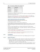
describes the bits and default settings of the
“Processor Bus Slave Image x Control Register”
Table 11: Programming Model for PB Slave Image Control Register
Bits
Type
Description
Default Setting
IMG_EN
R/W
Enables the PB slave image to decode in the specified
physical address range.
Disabled
TA_EN
R/W
Enables address translation (see
Slave Image x Translation Address Register” on
page 292
Disabled
BS[4:0]
R/W
Sets the block size of the PB slave image. The size of
the image is 4 Kbyte * 2
BS
.
Default value is 0. It can
be programmed through
any port after reset, or
loaded through
EEPROM.
MODE
R/W
Maps the incoming PB transaction to either Memory or
I/O space on the PCI bus.
Defaults to Memory
space.
DEST
R/W
Directs the incoming PB transaction to either of PCI-1
or PCI-2
Defaults to PCI-1
MEM_IO
R/W
Enables 1,2,3, or 4 byte memory reads on the PCI
bus(es).
Regular I/O mode
PRKEEP
R/W
Enables PowerSpan II to keep prefetch read data over
subsequent transactions.
Disabled
END[1:0]
R/W
Sets endian mapping to little-endian, PowerPC
little-endian, or big-endian
Big-endian is the default
mode.
RD_AMT[2:0]
R/W
Controls the prefetch read amount. Can be
programmed up to a maximum of 128 bytes.
8 bytes is the default
prefetch read amount
PB memory management supports a variety of memory/cache access attributes: write
through (W), caching-inhibited (I), and memory coherency (M). Although PowerSpan II
does not decode these attributes — external pins PB_GBL_ and PB_CI_ are output
only— specific guidelines must be followed to ensure correct system operation. These
guidelines are shown in
.
Table 12: Recommended Memory/Cache Attribute Settings
PowerSpan II Resource
Memory Coherency
Caching Inhibited
Registers
M=0
I=1
PCI I/O
space
M=0
I=1
PCI Memory space
M=0
External L2 cache: I=1
No External L2 cache: I=0 or 1


