background image

PIC32 Family Reference Manual

DS61104E-page 17-50

© 2007-2011 Microchip Technology Inc.

17.5.20 ADC Sampling Requirements


The analog input model of the 10-bit ADC module is shown in 

Figure 17-22

. The total acquisition 

time for the analog-to-digital conversion is a function of the internal amplifier settling time and the 
holding capacitor charge time.
For the ADC module to meet its specified accuracy, the charge holding capacitor (C

HOLD

) must 

be allowed to fully charge to the voltage level on the analog input pin. The analog output source 
impedance (R

S

), the interconnect impedance (R

IC

), and the internal sampling switch (R

SS

impedance combine to directly affect the time required to charge the C

HOLD

. The combined 

impedance of the analog sources must therefore be small enough to fully charge the holding 
capacitor within the chosen sample time. After the analog input channel is selected (changed), 
this acquisition function must be completed prior to starting the conversion. The internal holding 
capacitor will be in a discharged state prior to each sample operation.
A time period of at least 1 T

AD

 should be allowed between conversions for the acquisition time. 

Refer to the 

“Electrical Characteristics”

 section in the specific device data sheet for more 

information.

Figure 17-22: 10-bit ADC Analog Input Model 

17.5.21 Connection Considerations

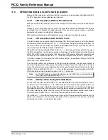
Since the analog inputs employ Electrostatic Discharge (ESD) protection, they have diodes to 
V

DD

 and V

SS

. This requires that the analog input must be between V

DD

 and V

SS

. If the input 

voltage exceeds this range by greater than 0.3V (in either direction), one of the diodes becomes 
forward-biased and it may damage the device if the input current specification is exceeded.
An external RC filter is sometimes added for anti-aliasing of the input signal. The R component 
should be selected to ensure that the acquisition time requirements are satisfied. Any external 
components connected (through high-impedance) to an analog input pin (capacitor, Zener diode, 
etc.) should have very little leakage current at the pin.

C

PIN

VA

Rs

ANx

V

T

 = 0.6V

V

T

 = 0.6V

I

LEAKAGE

R

IC


 250

Ω

Sampling

Switch

R

SS

C

HOLD

= DAC capacitance

V

SS

V

DD

= 4.4 pF

±

 500 nA

Note:

 The C

PIN

 value depends on the device package and is not tested. The effect of the C

PIN

 is negligible if Rs 

 5 k

Ω

.

R

SS


 3 k

Ω

Legend:

C

PIN

 = input capacitance

V

T

 = threshold voltage

R

SS

 = sampling switch resistance

R

IC

 = interconnect resistance

R

S

 = source resistance

C

HOLD

 = sample/hold capacitance

I

LEAKAGE

 = leakage current at the pin due to various junctions

Summary of Contents for AD1CHS

Page 1: ...ing major topics 17 1 Introduction 17 2 17 2 Control Registers 17 4 17 3 ADC Operation Terminology and Conversion Sequence 17 12 17 4 ADC Module Configuration 17 14 17 5 Miscellaneous ADC Functions 17...

Page 2: ...er to the specific device data sheet for more information The analog inputs are connected through two multiplexers to one SHA The analog input multiplexers can be switched between two sets of analog i...

Page 3: ...nverter ADC 17 Figure 17 1 10 bit High Speed ADC Block Diagram SAR ADC SHA ADC1BUF0 ADC1BUF1 ADC1BUF2 ADC1BUFF ADC1BUFE AN0 AN15 AN1 VREFL CH0SB 3 0 CH0NA CH0NB CH0SA 3 0 Channel Scan CSCNA Alternate...

Page 4: ...SAM ASAM SAMP DONE AD1CON2 1 2 3 31 24 23 16 15 8 VCFG 2 0 OFFCAL CSCNA 7 0 BUFS SMPI 3 0 BUFM ALTS AD1CON3 1 2 3 31 24 23 16 15 8 ADRC SAMC 4 0 7 0 ADCS 7 0 AD1CHS 1 2 3 31 24 CH0NB CH0SB 3 0 23 16 C...

Page 5: ...ult Word F ADC1BUFF 31 0 Table 17 1 ADC SFR Summary Continued Name Bit 31 23 15 7 Bit 30 22 14 6 Bit 29 21 13 5 Bit 28 20 12 4 Bit 27 19 11 3 Bit 26 18 10 2 Bit 25 17 9 1 Bit 24 16 8 0 Legend unimplem...

Page 6: ...000 0000 ssss sssd dddd dddd 000 Integer 16 bit DOUT 0000 0000 0000 0000 0000 00dd dddd dddd 111 Signed Fractional 32 bit DOUT sddd dddd dd00 0000 0000 0000 0000 110 Fractional 32 bit DOUT dddd dddd d...

Page 7: ...ts sampling When SSRC 000 writing 0 to this bit will end sampling and start conversion bit 0 DONE Analog to Digital Conversion Status bit 2 1 Analog to digital conversion is done 0 Analog to digital c...

Page 8: ...Read as 0 bit 10 CSCNA Scan Input Selections for CH0 SHA Input for MUX A Input Multiplexer Setting bit 1 Scan inputs 0 Do not scan inputs bit 9 8 Unimplemented Read as 0 bit 7 BUFS Buffer Fill Status...

Page 9: ...R W 0 R W 0 ADCS 7 0 1 Legend R Readable bit W Writable bit P Programmable bit r Reserved bit U Unimplemented bit n Bit Value at POR 0 1 x Unknown bit 31 16 Unimplemented Read as 0 bit 15 ADRC ADC Co...

Page 10: ...for MUX B 1 Channel 0 negative input is AN1 0 Channel 0 negative input is VR bit 30 28 Unimplemented Read as 0 bit 27 24 CH0SB 3 0 Positive Input Select bits for MUX B 1111 Channel 0 positive input is...

Page 11: ...es pin voltage Note 1 The AD1PCFG register functionality will vary depending on the number of ADC inputs available on the selected device Refer to the specific device data sheet for additional details...

Page 12: ...rolled manually or automatically The acquisition time may be started manually by setting the SAMP bit AD1CON1 1 and ended manually by clearing the SAMP bit in user software The acquisition time may be...

Page 13: ...dware sources or can be controlled manually in software by clearing the SAMP bit One of the conversion trigger sources is an auto conversion The time between auto conversions is set by a counter and t...

Page 14: ...7 4 7 6 Select the Scan mode using CSCNA AD1CON2 10 see 17 4 8 7 Set the number of conversions per interrupt SMP 3 0 AD1CON2 5 2 if interrupts are to be used see 17 4 9 8 Set Buffer Fill mode using BU...

Page 15: ...bits AD1CHS 27 24 and the negative input is controlled by the CH0NB bit AD1CHS 31 The positive input can be selected from any one of the available analog input pins The negative input can be selected...

Page 16: ...0 0 0 0 0 0 0 0 0 0 0 0 0 0 0 d09 d08 d07 d06 d05 d04 d03 d02 d01 d00 Signed Integer d09 d09 d09 d09 d09 d09 d09 d09 d09 d09 d09 d09 d09 d09 d09 d09 d09 d09 d09 d09 d09 d09 d09 d08 d07 d06 d05 d04 d03...

Page 17: ...d02 d01 d00 Read to Bus Integer 0 0 0 0 0 0 0 0 0 0 0 0 0 0 0 0 0 0 0 0 0 0 d09 d08 d07 d06 d05 d04 d03 d02 d01 d00 Signed Integer 0 0 0 0 0 0 0 0 0 0 0 0 0 0 0 0 d09 d09 d09 d09 d09 d09 d09 d08 d07...

Page 18: ...0000 0000 0000 0000 0 001 1 1024 00 0000 0001 0000 0000 0000 0000 0000 0000 0000 0001 1 1111 1111 1111 1111 1111 1110 0000 0001 511 0000 0000 0100 0000 0000 0000 0000 0000 0 001 1000 0000 0100 0000 0...

Page 19: ...C can be configured to automatically perform conversions at the rate selected by the SAMC 4 0 bits AD1CON3 12 8 The ADC is configured for this Trigger mode by setting the SSRC 2 0 bits to 111 In this...

Page 20: ...8 1 SCAN MODE ENABLE Scan mode is enabled by setting the CSCNA bit AD1CON2 10 When Scan mode is enabled the positive input of MUX A is controlled by the contents of the AD1CSSL register Each bit in t...

Page 21: ...erated This also defines the number of locations that will be written in the result buffer starting with ADC1BUF0 ADC1BUF0 or ADC1BUF8 for Dual Buffer mode This can vary from one sample to 16 samples...

Page 22: ...g to digital interrupt and the interrupt latency as determined by the application If the processor can unload a full buffer within the time it takes to sample and convert one channel the BUFM bit can...

Page 23: ...ADRC bit AD1CON3 15 1 the TAD is the period of the oscillator and no prescaler is used When using the internal oscillator the ADC can continue to function in Sleep mode and in Idle mode When the PBCLK...

Page 24: ...s shown in Equation 17 4 The ADC minimum requirements for TAD is met but not the sample time Equation 17 4 ADC Sample Plus Convert Time with a Minimum Sample Time b Increase the sample period to 2 TAD...

Page 25: ...imes for the sample and hold channel to acquire the analog signal The user must ensure the acquisition time meets the sampling requirements as outlined in 17 5 20 ADC Sampling Requirements When SSRC 2...

Page 26: ...her than manual 17 5 MISCELLANEOUS ADC FUNCTIONS 17 5 1 Aborting Sampling Clearing the SAMP bit AD1CON1 1 while in Manual Sample mode will terminate sampling but may also start a conversion if the SSR...

Page 27: ...sample sequence the number of samples as defined by the SMPI 3 0 bits AD1CON2 5 2 Hardware will the clear the ASAM bit AD1CON1 2 and set the inter rupt flag This will stop the sampling process to all...

Page 28: ...CON2 AD1CON3 AD1CHS AD1PCFG AD1CSSL Comparator 10 bit SAR Conversion Logic DAC AN12 AN13 AN14 AN15 AN8 AN9 AN10 AN11 AN4 AN5 AN6 AN7 AN0 AN1 AN2 AN3 Sample Control SHA ADC1BUF0 ADC1BUFF Control Logic...

Page 29: ...ADC Block Diagram for Scan Mode AD1CON1 AD1CON2 AD1CON3 AD1CHS AD1PCFG AD1CSSL Comparator 10 bit SAR Conversion Logic DAC AN12 AN13 AN14 AN15 AN8 AN9 AN10 AN11 AN4 AN5 AN6 AN7 AN0 AN1 AN2 AN3 Sample...

Page 30: ...1 AD1CON2 AD1CON3 AD1CHS AD1PCFG AD1CSSL Comparator 10 bit SAR Conversion Logic DAC AN12 AN13 AN14 AN15 AN8 AN9 AN10 AN11 AN4 AN5 AN6 AN7 AN0 AN1 AN2 AN3 Sample Control SHA ADC1BUF0 ADC1BUFF Control L...

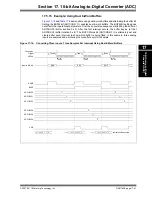
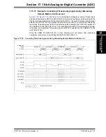
Page 31: ...g and starts conversion The user software must time the setting and clearing of the SAMP bit to ensure adequate acquisition time of the input signal See Example 17 1 for a code example Figure 17 8 Con...

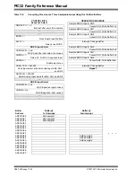
Page 32: ...ime as well as the acquisition time See Example 17 2 for a code example Figure 17 9 Converting 1 Channel Automatic Sample Start Manual Conversion Start Example 17 2 Converting 1 Channel Automatic Samp...

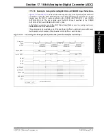
Page 33: ...st always be programmed for at least one clock cycle See Example 17 3 for a code example Figure 17 10 Converting 1 Channel Manual Sample Start TAD Based Conversion Start Example 17 3 Converting 1 Chan...

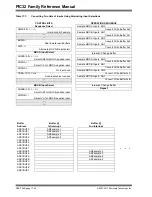
Page 34: ...sed Conversion Start Code ADCLK SAMP ADC1BUF1 TSAMP TCONV DONE 15 TAD TSAMP TCONV 15 TAD ADC1BUF0 set ASAM 1 Instruction Execution AD1PCFG 0xFFFB all PORTB Digital RB2 analog AD1CON1 0x00E0 SSRC bit 1...

Page 35: ...is set for automatic sampling and using a clocked conversion trigger the acquisition interval is determined by the SAMC 4 0 bits AD1CON3 12 8 Equation 17 11 shows the available sampling time Example 1...

Page 36: ...converting AD1CHS 0x00020000 Connect RB2 AN2 as CH0 input in this example RB2 AN2 is the input AD1CSSL 0 AD1CON3 0x0000 Sample time is TMR3 TAD internal TPB 2 AD1CON2 0x0004 Interrupt after 2 convers...

Page 37: ...peats 15 times until the buffer is full and then the module generates an interrupt The entire process repeats With the ALTS bit AD1CON2 0 clear only the MUX A inputs are active The CH0SA 3 0 bits AD1C...

Page 38: ...Inputs AN0 Convert Write Buffer 0x6 Sample MUX A Inputs AN0 Convert Write Buffer 0x7 Sample MUX A Inputs AN0 Convert Write Buffer 0x8 Sample MUX A Inputs AN0 Convert Write Buffer 0x9 Sample MUX A Inpu...

Page 39: ...s are similar to the previous example see 17 5 13 Sampling a Single Channel Multiple Times Initially the AN0 input is acquired and converted The result is stored in the ADC1BUF buffer Then the AN1 inp...

Page 40: ...A Inputs AN7 Convert Write Buffer 0x7 Sample MUX A Inputs AN8 Convert Write Buffer 0x8 Sample MUX A Inputs AN9 Convert Write Buffer 0x9 Sample MUX A Inputs AN10 Convert Write Buffer 0xA Sample MUX A...

Page 41: ...buffer at ADC1BUF0 buffer location 0 x 0 After the first interrupt occurs the buffer begins to fill at ADC1BUF8 buffer location 0 x 8 The BUFS Status bit AD1CON2 7 is alternately set and cleared after...

Page 42: ...nd AN2 MUX B Input Select CH0SB 3 0 n a MUX B positive input unused CH0NB n a MUX B negative input unused OPERATION SEQUENCE Sample MUX A Inputs AN0 Convert AN0 Write Buffer 0x0 Sample MUX A Inputs AN...

Page 43: ...t sample uses the MUX B inputs specified by the CH0SB AD1CHS 27 24 and CH0NB AD1CHS 31 bits In the following example one of the MUX B input specifications uses two analog inputs as a differential sour...

Page 44: ...e input OPERATION SEQUENCE Sample MUX A Inputs AN0 Convert Write Buffer 0x0 Sample MUX B Inputs AN1 Convert Write Buffer 0x1 Sample MUX A Inputs AN0 Convert Write Buffer 0x2 Sample MUX B Inputs AN1 Co...

Page 45: ...hen scanning is combined with Alternating Input mode the positive input to MUX A is selected by the contents of the AD1CSSL register not the CH0SA 3 0 bits AD1CHS 19 16 For each sample that MUX A is s...

Page 46: ...1CHS AD1PCFG AD1CSSL Comparator 10 bit SAR Conversion Logic VREF DAC AN12 AN13 AN14 AN15 AN8 AN9 AN10 AN11 AN4 AN5 AN6 AN7 AN0 AN1 AN2 AN3 VREF Sample Control SHA AVSS AVDD ADC1BUF0 ADC1BUFF Control L...

Page 47: ...n CSSL 15 0 n a Scan input select scan list consisting of AN0 and AN1 MUX B Input Select CH0SB 3 0 0010 Select AN7 for CH0 input CH0NB 0 Select VR for CH0 input OPERATION SEQUENCE Sample AN0 Convert W...

Page 48: ...The 00 0000 0001 code is centered at VR VR 1024 or 1 0 LSb The 10 0000 0000 code is centered at 512 VR VR 1024 An input voltage less than 1 VR VR L 2048 converts as 00 0000 0000 An input greater than...

Page 49: ...IC32 device package is shown as an example in Figure 17 21 Figure 17 21 ADC Voltage Reference Schematic VDD AVDD AVDD VDD R2 10 C2 0 1 F C1 0 01 F R1 10 C8 1 F VDD C7 0 1 F VDD C6 0 01 F VDD C5 1 F VD...

Page 50: ...on time Refer to the Electrical Characteristics section in the specific device data sheet for more information Figure 17 22 10 bit ADC Analog Input Model 17 5 21 Connection Considerations Since the an...

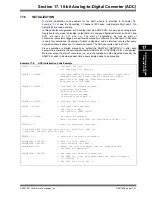
Page 51: ...sion i e end of acquisition is also triggered manually the SAMP bit needs to be cleared each time a new sample needs to be converted Example 17 6 ADC Initialization Code Example AD1PCFG 0x0000 Configu...

Page 52: ...ple RB2 AN2 is the input AD1CSSL 0 AD1CON3 0x0203 Sample time 2 TAD AD1CON2 0x6004 Select external VREF and VREF pins Interrupt after every 2 samples AD1CON1bits ADON 1 turn ON the ADC while 1 repeat...
Page 53: ...st priority to 0 the lowest priority An interrupt with the same priority group but having a higher subpriority value will preempt a lower subpriority interrupt that is in progress The priority group a...

Page 54: ...from the instruction after the WAIT instruction that placed the device in Sleep mode If the ADC interrupt is not enabled the ADC module will then be disabled although the ON bit AD1CON1 15 will remai...

Page 55: ...0 17 9 2 Power on Reset Following a Power on Reset POR event all of the ADC control registers AD1CON1 AD1CON2 AD1CON3 AD1CHS AD1PCFG and AD1CSSL are reset to a value of 0x00000000 This disables the AD...

Page 56: ...ts are pertinent and could be used with modification and possible limitations The current application notes related to the 10 bit Analog to Digital Converter ADC module are Title Application Note Usin...

Page 57: ...ns Added Equation 17 3 through Equation 17 9 in 17 4 12 1 Configuring the ADC for 1000 ksps Operation Figures Replaced Figure 17 1 Registers Removed all Interrupt registers Notes Removed Note 1 in Reg...

Page 58: ...PIC32 Family Reference Manual DS61104E page 17 58 2007 2011 Microchip Technology Inc NOTES...

Page 59: ...hip Technology Incorporated in the U S A All other trademarks mentioned herein are property of their respective companies 2007 2011 Microchip Technology Incorporated Printed in the U S A All Rights Re...

Page 60: ...China Shanghai Tel 86 21 5407 5533 Fax 86 21 5407 5066 China Shenyang Tel 86 24 2334 2829 Fax 86 24 2334 2393 China Shenzhen Tel 86 755 8203 2660 Fax 86 755 8203 1760 China Wuhan Tel 86 27 5980 5300...

Reviews: