© 2007-2011 Microchip Technology Inc.
DS61104E-page 17-23
Section 17. 10-bit Analog-to-Digital Converter (ADC)
10-b
it An
alog
-to
-Digit
a
l
Conve
rter (ADC)
17
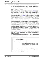
17.4.11.2 ALTERNATING INPUT SELECTIONS
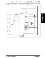
The ALTS bit (AD1CON2<0>) is used by the ADC module to alternate between the two input
multiplexers.
The inputs specified by the CH0SA<3:0> bits (AD1CHS<19:16>) and the CH0NA bit
(AD1CHS<23>) are called the MUX A inputs. The inputs specified by the CH0SB<3:0> bits
(AD1CHS<27:24>) and the CH0NB bit (AD1CHS<31>) are called the MUX B inputs.
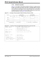
When the ALTS bit is ‘
1
’, the ADC module will alternate between the MUX A inputs on one sample
and the MUX B inputs on the subsequent sample. When the ALTS bit is ‘
0
’, only the inputs specified
by the CH0SA<3:0> and CH0NA bits are selected for sampling.
For example, if the ALTS bit is ‘
1
’ on the first sample/convert sequence, the inputs specified by
the CH0SA<3:0> and CH0NA bits are selected for sampling. On the next sample, the inputs
specified by the CH0SB<3:0> and CH0NB bits are selected for sampling. The pattern then
repeats.
17.4.12 Selecting the ADC Conversion Clock Source and Prescaler
The ADC module can use the internal RC oscillator or the Peripheral Bus Clock (PBCLK) as the
conversion clock source.
When the internal RC oscillator is used as the clock source (ADRC bit (AD1CON3<15>) =
1
), the
T
AD
is the period of the oscillator, and no prescaler is used. When using the internal oscillator the
ADC can continue to function in Sleep mode and in Idle mode.
When the PBCLK is used as the conversion clock source, the ADRC bit =
0
, the T
AD
is the period
of the PBCLK after the prescaler ADCS<7:0> bits (AD1CON3<7:0>) are applied.
The ADC has a maximum rate at which conversions may be completed. An Analog module clock,
T
AD
, controls the conversion timing. The analog-to-digital conversion requires 12 clock
periods (12 T
AD
).
The period of the ADC conversion clock is software selected using an 8-bit counter. There are
256 possible options for T
AD
, which are specified by the ADCS<7:0> bits (AD1CON3<7:0>).
gives the T
AD
value as a function of the ADCS bits and the device instruction cycle
clock period, T
CY
.
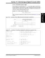
Equation 17-1:
ADC Conversion Clock Period
For correct analog-to-digital conversions, the ADC conversion clock (T
AD
) must be selected to
ensure a minimum T
AD
17.10 “Related Application Notes”
).
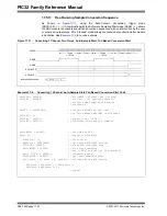
Equation 17-2:
Available Sampling Time, Sequential Sampling
Note:
The internal RC oscillator is intended for ADC operation in Sleep mode, and
therefore, it is not calibrated. Applications requiring precise timing of ADC
acquisitions should use a stable calibrated clock source for the ADC.
T
AD
2
T
PB
ADCS
1
+
(
)
•
(
)
•
=
ADCS
T
AD
2
T
PB
•
------------------
⎝
⎠
⎛
⎞
1
–
=
T
SMP
TriggerPulseInterval T
SEQ
(
)
ConversionTime T
CONV
(
)
–
=
T
SMP
T
SEQ
T
CONV
–
=
Note:
T
SEQ
is the trigger pulse interval time.

