4-16
MPC8240 Integrated Processor User’s Manual
PCI Interface Configuration Registers
4.2.8 PCI Interrupt Line—Offset 0x3C
Table 4-13 describes the PCI interrupt line register (ILR).
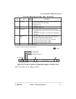
4.2.9 PCI Arbiter Control Register (PACR)—Offset 0x46
This register controls the on-chip arbitration for external PCI masters. As many as five
external devices are supported.
Table 4-13. Interrupt Line Register—0x3C
Bits Reset
Value
Description
msb 7–0
0x00
Contains the interrupt routing information. Software can use this register to hold
information regarding on which input of the system interrupt controller corresponds to the
INTA signal. Values in this register are system-architecture-specific.
Table 4-14. PCI Arbiter Control Register Bit Definitions—0x46
Bits
Reset
Value
R/W
Description
msb
15
x
R/W
Enable on-chip PCI arbitration
0 If cleared, the on-chip arbiter for external PCI masters is disabled, and the MPC8240
presents its request on GNT0 to the external arbiter and receives its grant on REQ0.
1 If set, indicates the on-chip arbiter is enabled.
14–13
00
R/W
Parking mode controls which device receives the bus grant when there are no outstanding
bus requests and the bus is idle.
00 The bus is parked with the last device to use the bus.
01 The bus is parked with the device using REQ0 and GNT0.
10 The bus is parked with MPC8240.
11 Reserved; do not use.
12
0
R/W
PCI broken master disable. This bit controls whether the PCI arbiter negates the bus grant
to a requesting master that does not assert FRAME within 16 PCI clock cycles from the
time the bus is idle.
0 PCI arbiter negates the PCI GNTx signal to a requesting master that does not begin
using the bus (by asserting FRAME) within 16 PCI clock cycles from the time the PCI
clock is idle.
1 A PCI master that has been granted the bus never loses its grant until (and unless) it
begins a transaction or negates the REQx signal.
It is recommended that this bit stay cleared.
11
0
R
Reserved
10
0
R/W
Retry PCI Configuration Cycle
1 PCI target logic retries all external PCI configuration transactions.
0 PCI target logic responds to external PCI configuration transactions.
9–8
00
R
Reserved
7
0
R/W
MPC8240 priority level, 1 = high, 0 = low
6–5
00
R
Reserved
4–0
0_0000
R/W
External device priority levels, 1 = high, 0 = low. Bit 0 corresponds to the device using
REQ0 and GNT0, bit 1 to REQ1 and GNT1, etc.
Summary of Contents for MPC8240
Page 1: ...MPC8240UM D Rev 1 1 2001 MPC8240 Integrated Processor User s Manual ...
Page 38: ...xviii MPC8240 Integrated Processor User s Manual TABLES Table Number Title Page Number ...
Page 48: ...xlviii MPC8240 Integrated Processor User s Manual Acronyms and Abbreviations ...
Page 312: ...6 94 MPC8240 Integrated Processor User s Manual ROM Flash Interface Operation ...
Page 348: ...7 36 MPC8240 Integrated Processor User s Manual PCI Host and Agent Modes ...
Page 372: ...8 24 MPC8240 Integrated Processor User s Manual DMA Register Descriptions ...
Page 394: ...9 22 MPC8240 Integrated Processor User s Manual I2O Interface ...
Page 412: ...10 18 MPC8240 Integrated Processor User s Manual Programming Guidelines ...
Page 454: ...12 14 MPC8240 Integrated Processor User s Manual Internal Arbitration ...
Page 466: ...13 12 MPC8240 Integrated Processor User s Manual Exception Latencies ...
Page 516: ...16 14 Watchpoint Trigger Applications ...
Page 538: ...B 16 MPC8240 Integrated Processor User s Manual Setting the Endian Mode of Operation ...
Page 546: ...C 8 MPC8240 Integrated Processor User s Manual ...
Page 640: ...INDEX Index 16 MPC8240 Integrated Processor User s Manual ...


