

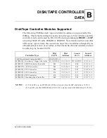


Disk/Tape Controller Data
B-2
MVME166 Single Board Computer Installation Guide
B
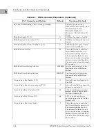
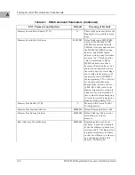
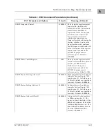
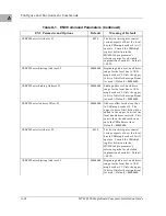
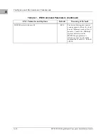
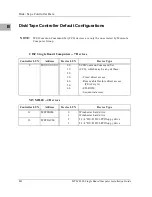
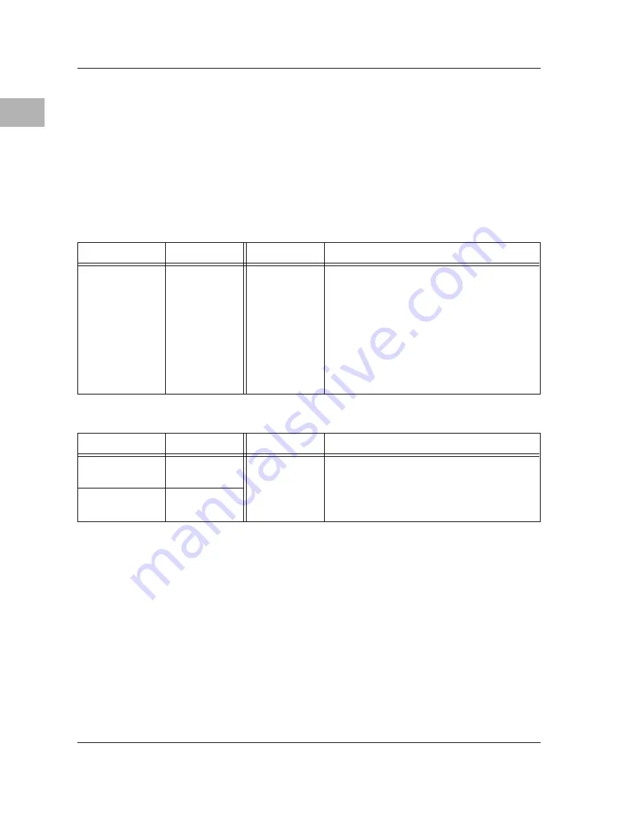
Disk/Tape Controller Default Configurations
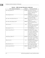
CISC Single Board Computers -- 7 Devices
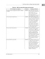
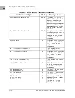
MVME320 -- 4 Devices
NOTE:
SCSI Common Command Set (CCS) devices are only the ones tested by Motorola
Computer Group.
Controller LUN
Address
Device LUN
Device Type
0
$XXXXXXXX
00
10
20
30
40
50
60
SCSI Common Command Set
(CCS), which may be any of these:
- Fixed direct access
- Removable flexible direct access
(TEAC style)
- CD-ROM
- Sequential access
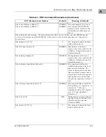
Controller LUN
Address
Device LUN
Device Type
11
$FFFFB000
0
1
2
3
Winchester hard drive
Winchester hard drive
5-1/4" DS/DD 96 TPI floppy drive
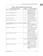
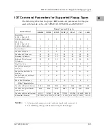
12
$FFFFAC00
5-1/4" DS/DD 96 TPI floppy drive
Summary of Contents for MVME166
Page 1: ...MVME166 Single Board Computer Installation Guide MVME166IG D2 ...
Page 12: ...xii ...
Page 14: ...xiv ...
Page 46: ...Hardware Preparation and Installation 2 10 MVME166 Single Board Computer Installation Guide 2 ...
Page 70: ...Debugger General Information 3 24 MVME166 Single Board Computer Installation Guide 3 ...
Page 114: ...Disk Tape Controller Data B 6 MVME166 Single Board Computer Installation Guide B ...
Page 116: ...Network Controller Data C 2 MVME166 Single Board Computer Installation Guide C ...


