Defining the I/O Map
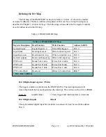
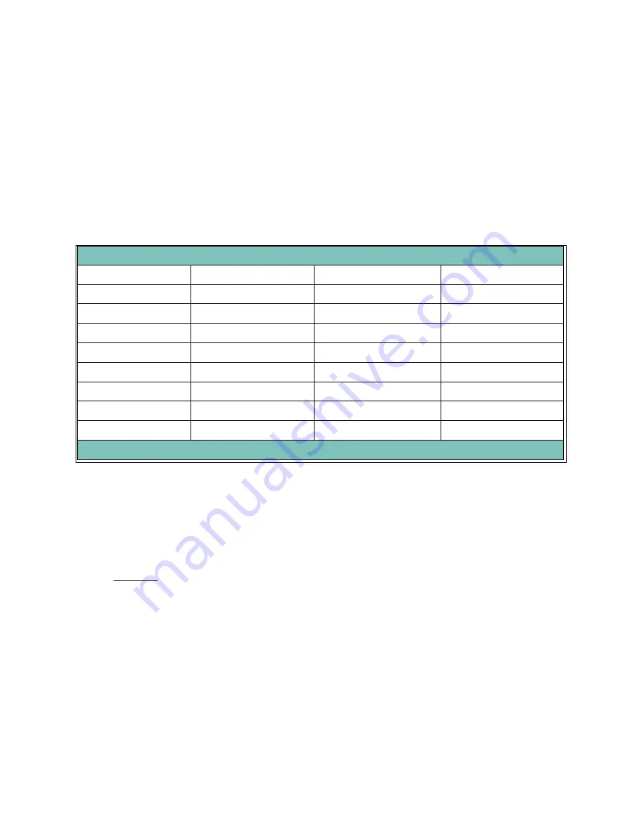
The I/O map of the DM6854HR is shown in Table 4-1 below. As shown the module
occupies 8 addresses. The Base Address (designated as BA) can be set using the jumpers as
described in Chapter 1, Module Settings. The following sections describe the register contents
of each address used in the I/O map.
Table 4-1 DM6854HR I/O Map
Table 4-1 DM6854HR I/O Map
Register Description
Read Function
Write Function
Address in HEX
Isolated inputs
Digital Inputs 1-8
Clear IRQ (trigger)
BA+0
Input Mask
Read input mask
Write to mask register
BA+1
Input Inversion
Read input inv. reg.
Write to input inv. reg.
BA+2
Isolated outputs
Read conf/output reg. Write conf/output reg
BA+3
PPI Port A
Reads Port A data
Writes Port A data
BA+4
PPI Port B
Reads Port B data
Writes Port B data
BA+5
PPI Port C
Reads Port C data
Writes Port C data
BA+6
PPI Control Byte
Reserved
Writes to Control byte
BA+7
* BA = Base Address
BA+0 Digital input register (Write)
The trigger condition is latched on the DM5854/6854. The interrupt request will
remain high until the host acknowledges the interrupt. This is done with a write to BA+0.
Example:
outp(BA,data);
// Clears trigger and interrupt; data is irrelevant.
BA+0 Digital inputs
(Read)
The eight isolated digital input bits available in connector J4 can be read from address
BA+0.
DM5854HR/DM6854HR Page 29 (c) RTD Finland Oy 1996-2001


