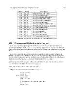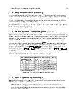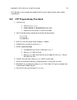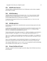
• OTP Memory must be programmed
only
while the power supply voltages remain within
specification.
1. LOCK the otp:
a. Write 0x1 to
otp_lock
b.
Check that 0x1 is read back from
otp_lock
.
c. Repeat this step until 0x1 is read successfully.
2. SET the programming voltages by writing the following values:
otp_mrr=0x4
otp_mpp=0x0
otp_vppen=0x0
3. WAIT 20 us for the programming voltages to stabilize.
4. ADDRESS the memory by setting
otp_a
.
5. WRITE
one bit at a time
:
a. Set
only
the bit you want to write high in
otp_d
b. Bring
otp_ck
HIGH for 50 us
c. Bring
otp_ck
LOW. Note that this means
only
one bit of
otp_d
should
be high at any time.
6. VERIFY the written bits setting
otp_mrr
=0x9 for read margin.
7. SOAK any verification failures by repeating steps 2-5 using 400 us pulses.
8. REVERIFY the rewritten bits setting
otp_mrr
=0xF. Steps 7,8 may be repeated up to
10 times before failing the part.
9. UNLOCK the otp by writing 0x0 to
otp_lock
.
Copyright © 2019, SiFive Inc. All rights reserved.
55
Summary of Contents for FE310-G002
Page 1: ...SiFive FE310 G002 Manual v19p05 SiFive Inc ...
Page 11: ...Figure 1 FE310 G002 top level block diagram Copyright 2019 SiFive Inc All rights reserved 9 ...
Page 15: ...Chapter 2 List of Abbreviations and Terms 13 ...
Page 23: ...Chapter 4 Memory Map The memory map of the FE310 G002 is shown in Table 4 21 ...


