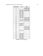
FE310-G002 contains one GPIO instance. Its address and parameters are shown in Table 51.
Instance Number
Address
ngpio
0
0x10012000
32
Table 51:
GPIO Instance
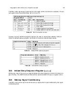
The memory map for the GPIO control registers is shown in Table 52. The GPIO memory map
has been designed to require only naturally-aligned 32-bit memory accesses. Each register is
ngpio
bits wide.
Offset
Name
Description
0x00
input_val
Pin value
0x04
input_en
Pin input enable*
0x08
output_en
Pin output enable*
0x0C
output_val
Output value
0x10
pue
Internal pull-up enable*
0x14
ds
Pin drive strength
0x18
rise_ie
Rise interrupt enable
0x1C
rise_ip
Rise interrupt pending
0x20
fall_ie
Fall interrupt enable
0x24
fall_ip
Fall interrupt pending
0x28
high_ie
High interrupt enable
0x2C
high_ip
High interrupt pending
0x30
low_ie
Low interrupt enable
0x34
low_ip
Low interrupt pending
0x40
out_xor
Output XOR (invert)
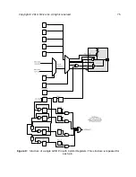
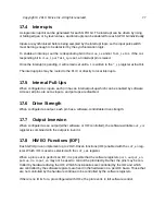
The GPIO can be configured on a bitwise fashion to represent inputs and/or outputs, as set by
the
input_en
and
output_en
registers. Writing to the
output_val
register updates the bits
regardless of the tristate value. Reading the
output_val
register returns the written value.
Reading the
input_val
register returns the actual value of the pin gated by
input_en
.
Table 52:
GPIO Peripheral Register Offsets. Only naturally aligned 32-bit memory accesses
are supported. Registers marked with an * are asynchronously reset to 0. All other registers are
synchronously reset to 0.
Copyright © 2019, SiFive Inc. All rights reserved.
76
Summary of Contents for FE310-G002
Page 1: ...SiFive FE310 G002 Manual v19p05 SiFive Inc ...
Page 11: ...Figure 1 FE310 G002 top level block diagram Copyright 2019 SiFive Inc All rights reserved 9 ...
Page 15: ...Chapter 2 List of Abbreviations and Terms 13 ...
Page 23: ...Chapter 4 Memory Map The memory map of the FE310 G002 is shown in Table 4 21 ...


